Graphene is a zero-band gap semiconductor and has emerged as a promising candidate for device application due to its superior electrical performance [1-5]. Despite the good potential as channel material for field effect transistors (FETs), the contact resistance between metal and graphene can be a major limiting factor of device performance [6-8]. Therefore, understanding the metal-graphene contact is of great scientific and technological importance. Carrier transport from a three dimensional metal to two dimensional graphene has a different mechanism from the conventional metal-metal contact [9]. However, in spite of its importance, there have been few reports on understanding the dominant factors that control the contact resistance between graphene and metal. The detailed properties and methods to improve the contact between graphene and metal are not well studied. Here we demonstrate a new method to reduce the contact resistance between transferred graphene and metal using chemical vapor deposition (CVD) grown graphene as an intermediate layer. In a conventional graphene-metal contact, a transferred graphene layer contacts metal. In our approach, however, there is another synthesized graphene layer between the metal and graphene, which can reduce the contact resistance between them.
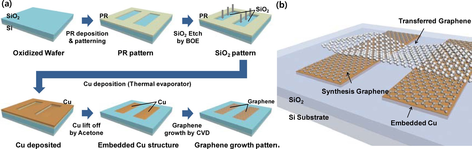
In our new approach, a synthesized graphene layer on top of the metal was used underneath the transferred graphene for a FET channel. In a conventional graphene transistor, metal electrodes are deposited on top of the transferred graphene placed on a substrate, which is usually SiO2/Si. In this approach, however, an embedded metal electrode structure is used to insert the graphene intermediate layer between the metal-graphene contacts. The Cu is used as an embedded electrode, which is widely used as catalyst metal for the graphene synthesis by CVD growth [10,11]. The overall process of fabricating the embedded Cu electrode structure is summarized in Fig. 1a. To make space for the Cu electrode, 1-μm-thick SiO2 was etched by BOE after surface
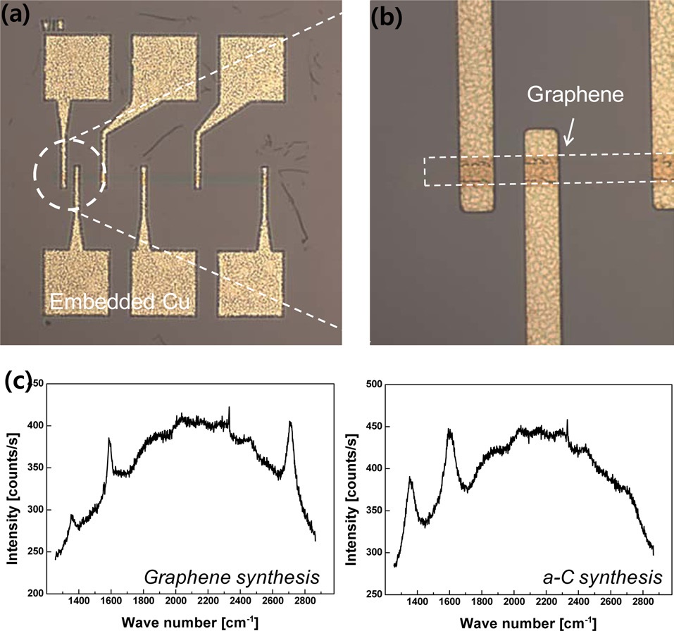
patterning. The Cu electrode was then deposited by thermal evaporation and lifted off to eliminate Cu on SiO2. A graphene intermediate layer was grown on the embedded Cu electrodes by induction coupled plasma enhanced CVD (ICP-CVD). The substrate temperature was ramped up to 850℃, and C2H2 gas was supplied to a chamber with plasma, which decomposed the C2H2 gas to carbon source for graphene deposition. Then the substrate was cooled to room temperature in vacuum conditions. Another graphene layer as a channel material for a FET, which was grown separately on another Cu/SiO2/Si wafer, was transferred onto the substrate, which is illustrated in Fig. 1b. To confirm the growth of the graphene intermediate layer, Raman spectroscopy was used and prominent G and 2D peaks showed that the carbon film on the metal was truly graphene (Fig. 2c).
The metal-graphene contact resistance was measured using transfer length methods (TLM) [12-14] and a TLM device is shown in Fig. 2a. The graphene channel width was 10 μm and the channel length varied from 2 μm to 10 μm in steps of 2 μm and a top gate was fabricated in one of the TLM segments with a 20-nm-thick Al2O3 dielectric and Au as the top gate material (the top gate is not shown in the figure). The graphene intermediate layer was synthesized only on the Cu electrodes and bar-shaped graphene as a channel was placed on them. For comparison, not only graphene but also an amorphous carbon (a-C) film was synthesized as an intermediate layer and the Raman spectroscopy measurement result is shown in Fig. 2c.
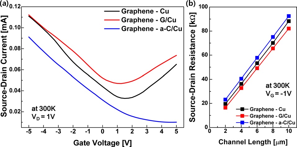
We conducted three different tests, TLM measurement, Hall effect measurement, and a cantilever beam fracture test, to access the electronic and mechanical performances of the intermediate layer. First, we made TLM measurements at 300 K with a drain bias of 1 V on three different structures, Cu/transferred graphene contact (called direct contact), Cu/intermediate graphene/transferred graphene (indirect contact), and Cu/amorphous carbon/transferred graphene (amorphous contact). The drain current-gate voltage (I-V) characteristics of all of the top gate graphene FETs are plotted in Fig. 3a as a function of top-gate bias for all three different types of FETs. The highest source-drain current was from the indirect contact. The total resistance (Rtotal) between a source and a drain electrode includes contact and sheet resistances, and its dependence on the channel length is plotted in Fig. 3b. The Rtotal was measured at a gate bias of -1 V. The black (red, blue) squares denote the Rtotal of the FETs having direct (indirect, amorphous) contact and the lines are linear fitting curves. The resistance values increased with the channel length as expected. However, the contact resistance was constant regardless of the channel length, and the value was obtained at the intercept at the zero channel length.
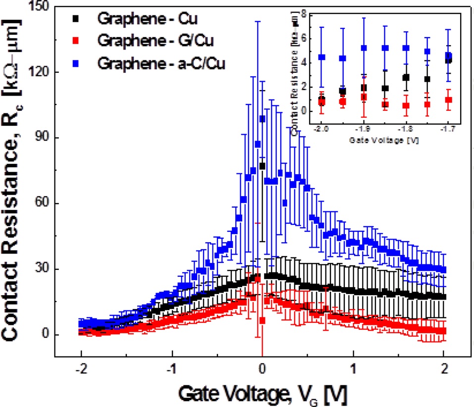
The measured contact resistance is plotted in Fig. 4. Note that the error bars are significantly larger near Vdirac due to the large resistance used in extrapolation around Vdirac, leading to larger absolute errors despite the high fit quality. Moreover, near Vdirac, Rtotal changes rapidly and a slight variation in Vdirac across all different structures leads to additional errors. We measured more than 20 FETs for each type of contact and consistent results were obtained. The smallest contact resistance was observed in the indirect contact. When the gate voltage was applied in the range of -2.0 V to -1.7 V far away from the Vdirac, the contact resistances did not vary significantly as shown in the inset of Fig. 4, and their values are similar to reported values [15]. The contact resistances of the proposed structure, indirect Cu-graphene contact by a graphene intermediate layer, had less
than half the value of the direct Cu-graphene throughout most of the investigated gate voltages. That means that the intermediate layer assisted the charge transfer from Cu to the transferred graphene. In the amorphous contact, the contact resistance was over the 4 kΩ- μm because the charge transfer was harder than the other structures due to low conductivity of the amorphous carbon film.
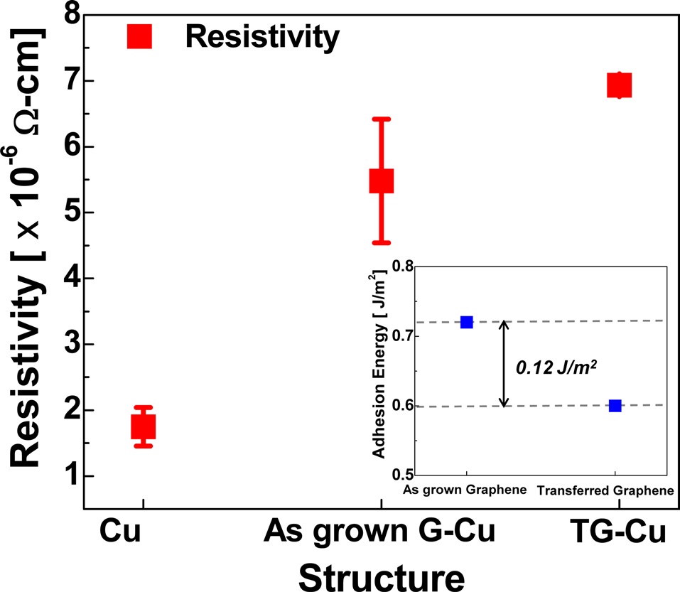
As another test method for the electrical performance enhancement and the adhesion property, we used Hall effect measurements and cantilever beam fracture measurement. For the electrical contact analysis, resistivity of Cu, CVD grown graphene on Cu, and transferred graphene on Cu had been measured by the Hall Effect measurement (Fig. 5). The resistivity of the grown graphene on Cu was lower than the transferred one, and it was closer to the pure Cu value. The adhesion energy between graphene and Cu was measured by double cantilever beam fracture mechanics testing with a high-precision micromechanical test system (Delaminator Adhesion Test System; DTS Company, MenloPark, CA, USA) [16]. The transferred graphene and Cu had 0.6 J/m2 adhesion energy, while the CVD graphene had 0.72 J/m2 adhesion energy in the Fig. 5 inset. The
CVD grown graphene had harder contact with Cu than the transferred graphene, which can make the electric current easy to turn on. From these results, we conclude that CVD grown graphene has better surface contact than transferred graphene.
In summary, we proposed a new contact structure to reduce contact resistance by inserting a graphene intermediate layer between the metal and the transferred graphene. Using TLM, Halleffect, and adhesion tests, we verified that CVD grown graphene has lower resistivity and higher adhesion energy than transferred graphene on Cu. The proposed structure decreases nearly half the contact resistance. The results indicate that CVD grown graphene is more strongly contacted with Cu than the transferred graphene, which makes the charge transfer more effective between the electrode and the channel.