Since the first demonstration of top-gated graphene transistor in 2007 [1], there has been major progress in the development of graphene devices, especially radio-frequency transistors [2-18]. The most of the improvement was achieved by the development of the gate oxide deposition process, exemplified by inserting interfacial layers or thin Al film before the atomic layer deposition process [5,19,20]; the formation of relatively low contact resistance with Pd or Ti [21,22], or the implementation of short-channel devices by a self-alignment process [10,16,17,23,24]. Although significant advances in terms of performance have been made, the contact resistance is still poorly understood despite the fact that it is one of the most critical barriers preventing further improvements [21,25-33]. In this paper, a short review of the properties of graphene-metal contacts is given. The contents include work function pinning as induced by a metal contact, charge transport at the contact region, and a discussion of the impact of the process conditions on the characterization process. It should be emphasized that the dominant factors which significantly determine the intrinsic contact resistance have not been clearly identified. To exploit the superior electrical properties of graphene fully, a reliable and the reproducible metal contact process scheme must be developed in the future.
2. The work function pinning of graphene under metal
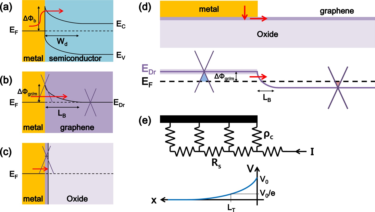
When a metal and a semiconductor come into contact, charges are transferred from higher energy states to lower energy states until the energy levels are balanced in an equilibrium state. Due to the small density of states in a semiconductor, there is energy band bending along the vertical direction, as shown in Fig. 1a, in what is known as the depletion region with depletion width Wd. In a similar manner, graphene can also be modeled as a semiconductor with a zero band gap, and band bending is necessary if graphene has a finite thickness as a bulk semiconductor materials. Because graphene has no band gap, instead of an ‘energy band,’ the ‘Dirac energy level’ (EDr) would be a proper term for graphene, as illustrated in Fig. 1b. Dirac energy level bending in graphene along the lateral direction does not occur, but there is a work function shift in graphene (Fig. 1c). It was first theoretically estimated that graphene on various crystalline metals can be doped due to the presence of an interface
dipole layer induced by the charge transfer [34]. The metals were classified in two types, and the characteristics of graphene were found to be significantly altered by chemisorption on Co, Ni, and Pd. In contrast, graphene weakly bonds to Al, Cu, Ag, Au, and Pt and preserves its conical electronic structure. The weak bonding leads to a work function shift in graphene, and the amount of this shift is determined by the work function of the corresponding metal.
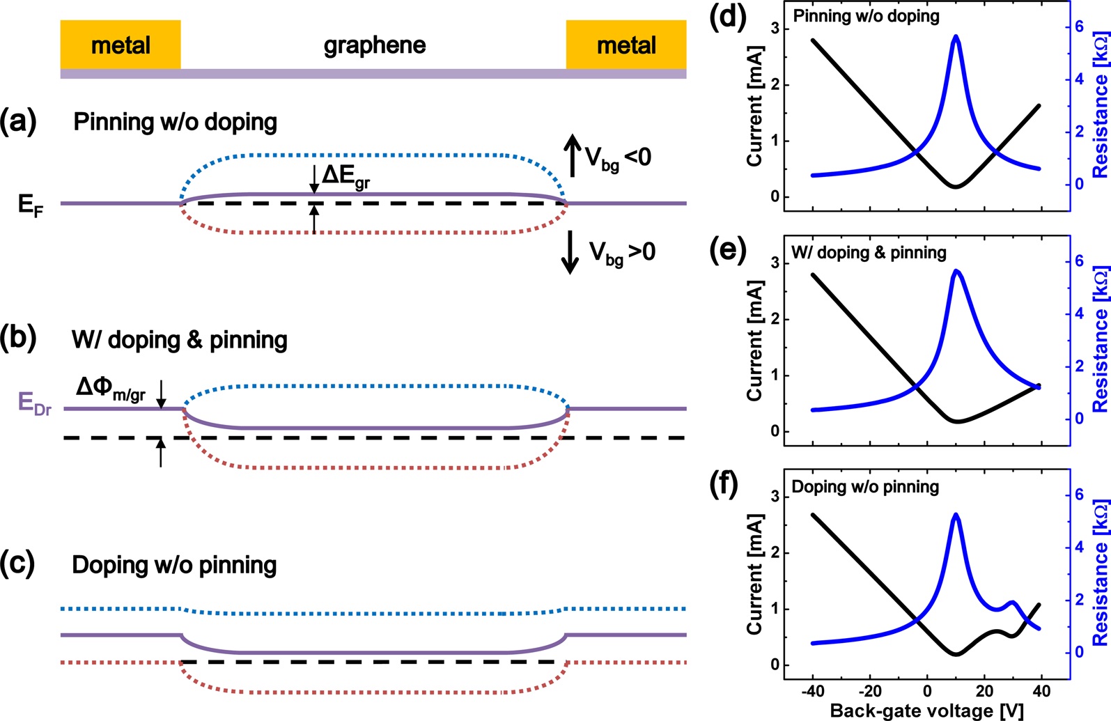
In addition to the shift of the work function of graphene underneath metal, there is a gradual bending of the Dirac energy level along the horizontal direction near the contact edge due to the work function difference between the exposed graphene and the graphene underneath the metal, as shown in Fig. 1d [35]. This region, known as the charge transfer region, has been successfully measured by Kelvin probe force microscopy [36,37], and photocurrent experiments [38-41]. Clear Dirac energy level shifts have been observed near the edge of the graphene?metal contact, and metal-induced work function pinning has also been clearly identified. The presence of a charge transfer region leads to the formation of a p-n junction in the graphene channel, which increases the resistance in graphene compared to a p-p’ or n-n’ junction [42]. This introduces important electrical characteristics in graphene, such as asymmetric conductance behaviour coupled with back?gate voltage dependence [21,25,42-44]. It also leads to errors during the determination of the sheet resistance and contact resistance during transmission length measurements (TLM) or four-point probe measurements (see the details in Section 4) [43,45]. Fig. 2 shows schematic illustrations of the energy band bending and electrical characteristics with the back gate voltage. If there is no metal-induced doping and if the work function at the contact region is independent of the back gate voltage, the VG-ID characteristic curve will show symmetry, as depicted in Fig. 2d. In contrast, the curve is asymmetric with respect to the Dirac voltage and the hole current is usually higher than the electron conductance when a contact is formed by Pd or Ni [21,41,44,46]. This indicates that the work function of graphene under the corresponding metal is pinned to a higher value than its original work function (that of the exposed graphene), and higher resistance is observed when the external field lowers the Dirac energy level of the channel below Fermi level, thereby leading to the formation of a p-n junction, as illustrated in Figs. 2b and e.
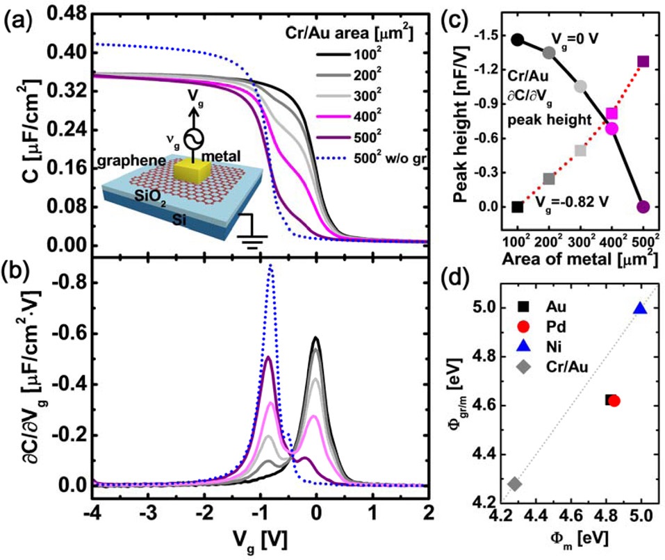
To understand the detailed carrier transport behavior of graphene field-effect transistors (FETs), the precise work function of graphene under metal is one type of basic information. Previously reported values measured by scanning photocurrent microscopy were evaluated from indirect measurements, e.g., by finding the gate voltage that yields a flat channel potential profile [38-41]. As the flat band voltage (
function of graphene under a noble metal was measured to be ~4.62 eV, as shown in Fig. 3c, and this is in good agreement with the previously reported values of the potential step at the graphene/ Pd interface (approximately 95~120 m
3. Charge transport in contact
Carrier transport in a graphene-metal contact system is understood to take place in two cascading steps. Charges in the metal are first injected into the underlying graphene and then flow towards the graphene channel [21]. The former step is significantly affected by the contact metal species and the metallization process. The interaction between the graphene and metal, the work function of the graphene, or residues at the interface are crucial factors determining the transmission of charges at the interface. The injected carriers then face a built-in potential barrier, the charge transfer region, formed by the pinning of the work function in graphene due to the metal contact as noted in the previous section. The interfacial potential barrier width, shape, and
height can crucially affect the carrier tunneling probability [21]. In addition to the two interfaces, the conduction modes of both the graphene at the channel and the contact region contribute to the contact resistance. Therefore, the lowest number of modes between them and the carrier transmission probability at the two interfaces determine the overall contact conductance.
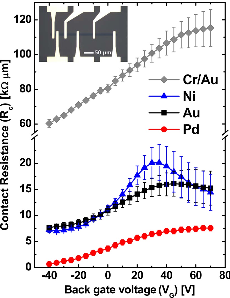
As the conduction mode of graphene contributes to the properties of the contact, the contact resistance shows gate-dependent behavior, as shown in Fig. 4. Similar to the bell-shaped resistance of graphene as a function of the gate voltage, the contact resistance also reaches its maximum value near the Dirac voltage due to the absence of a conduction mode in the channel. In contrast to the channel, it is not clearly understood if the conduction mode of graphene underneath a metal contact can be modulated by back gate bias. The number of peaks in the contact resistance (or the channel resistance) offer a clue about the modulation of the density-of-state (DOS) in graphene at the contact region, as shown in Figs. 2c and f [21,41]. In a simple situation without charge puddles in the channel and the broadening of DOS in the contact region, if graphene at the contact and channel region can be modulated by the back gate bias and if each has a different energy difference between the Fermi level and Dirac point energy, the contact resistance will exhibit two peaks. One of them originates from the minimum DOS in the channel and the other peak corresponds to the minimum DOS in the graphene at the contact. The single peak in the contact resistance measured as a function of the back gate voltage indicates that graphene underneath metal cannot be modulated by the bias. Most reports on the contact resistance measured with the back gate voltage have shown a single peak, indicating that the metal-induced pinning of the work function of graphene is independent of the external field.
The determination of a single peak in the contact resistance is not easy in real situations. One of the reasons is the large standard deviation of the contact resistance near the Dirac voltage, leading to an unclear position of the peak or an ambiguous situation when attempting to count the number of peaks. Such larger error bars originates from the charge puddles in graphene at the channel or the contact, or for instance by the extraction method. More details about the larger distribution of the contact resistance are given in Section 4. The larger broadening energy in the contact region also makes the peaks vague and makes it difficult to identify the presence of peaks [21]. In addition, the broadening of DOS in the graphene channel results in the broadening of the peak, making the separation of the peaks difficult. There are, however, few reports on the modulation of DOS in graphene underneath metal. The asymmetric transfer characteristics of fully covered top-gated graphene FETs have been explained in terms of the impact of the back-gate bias on the Fermi level shift in the graphene under the metal [41,46,50]. Chen and Appenzeller [46] also suggested that the energy dispersion of graphene underneath metal can be altered due to the much lower dependence on the back-gate bias. The similar broadening of the DOS of graphene at the contact area has been introduced to explain the observation of a single minimum during asymmetric conductance [51]. From simulation results in the referenced study, it was estimated that the transfer characteristics will have two minima when the energy dispersion of graphene in the contact region is intrinsic and the Fermi level is not aligned with that of the channel graphene, as two the Dirac levels in both the channel and contact region can be modulated together with back-gate bias. Interestingly, two minima have been measured from Ni-contacted FETs, indicating the free of metal-induced pinning, and it has been suggested that the oxidation of the metal surface occurs at the contact interface [44]. It was noted that the amount of the modulation of DOS in the graphene at the contact region can differ from that in the channel due to the different coupling ratio contributed by the metal [50]. As the coupling ratio at the contact is wholly determined by the graphene-metal interaction, the distance between the graphene and the metal, the metal-induced broadening, and the inhomogeneous broadening may determine the amount of modulation at the contact region [21]. Because the influence of the back-gate voltage on the work function pinning of graphene underneath the metal can play a critical role in the operation of the device, clearer and direct evidence must be identified in the future.
At a high negative or positive back-gate bias with respect to the Dirac voltage, the conduction mode of the channel is large enough and the contact resistance is determined by the charge transmittance at the two interfaces and the DOS of the graphene at the contact point. A higher conduction mode or higher work function difference as regards the Fermi level of the graphene underneath the metal is expected to show lower contact resistance [21]. It has been found, however, that a higher work function of graphene does not guarantee lower contact resistance [47]. Ni contact results in the work function of graphene exceeding 5 eV, but the contact resistance is about 10 times higher compared to a Pd contact in a high-bias regime. This indicates that the work function of graphene underneath metal is not a critical factor affecting the contact resistance.
One of the possible reasons for the non-critical contribution of the work function may be the current crowding effect [25,52]. During graphene-metal contact, the charges flow within a finite length at the edge and the contact resistance is a linear function of the width of the metal, but not a function of the length of the metal on the graphene [25]. The transfer length, which is the length at the potential decreases to e-1 from the edge, as shown in Fig. 1e, is known to be shorter than 1 μm [25,31]. The transfer length with a Pd contact has been found to range from 50 to 250 nm [21], while that with Ti contact reaches only about 200 nm [53]. It was noted that such a short Lt leads to current crowding at the contact edge, which generates local heating and results in degraded contact performance or undesirable electrical properties such as an increase in 1/f noise [52,54].
The carrier transport at the p-p’ and n-n’ interfacial built-in potential is known to be nearly transparent due to Klein tunneling [21,55,56]. In contrast, transmission through the p-n junction undergoes relatively high resistance, as explained previous section. The charge transfer through the interfacial barrier in graphene at the contact edge has been analyzed with various potential profiles [21]. In addition to exponential potential profiles, linear, 1/
Carrier transport at metal-graphene junctions was thoroughly investigated in an earlier study [21]. The injection efficiency at the interface has been classified into two regimes: one characterized by the diffusive transport limit and the other by the ballistic transport limit. Regarding the ballistic transport limit, where the scattering mean-free path is longer than the graphene-metal coupling length, the injection efficiency is expected to be close to one and the Pd contact is estimated to exhibit transmission efficiency of around 75%, indicating the ballistic transport type. The graphene-metal coupling length can be strongly affected by the interaction between the π-orbitals in graphene and the metal d-states. Therefore, the graphene-metal distance, wettability, or the deformation potential due to the metal contact can play significant roles in the coupling length. In terms of the graphene- metal distance, Ti is expected to show the lowest contact resistance as compared to Pd, Pt, Cu, and Au [57]. On the other hand, utilizing higher quality graphene, which exhibits higher mobility and less scattering, leads to the longer mean-free path. In addition, the scattering mean-free path can also be affected by phonon interaction and by coulomb scattering with the supporting substrate. Among the various treatments on SiO2, the O2 plasma treatment on SiO2 results in stronger interaction with graphene compared to Ar or H2 gas treatments, leading to degraded mobility. It has been reported that HF-dipped SiO2 shows smaller hysteresis and higher mobility compared to other treatment processes such as that with O2 plasma or re-oxidation. Different substrates also cause different doping states in graphene [58,59]. These results indicate that the interaction between graphene and substrate can strongly affect the contact properties and the graphene-metal interaction.
4. Process dependence on the contact resistance
At an early stage of study on contact resistance in graphene FETs, no gate voltage dependence was thought to exist [29,30]. However, strong dependence on the gate bias was noted, sometimes even showing negative values [19,21,26,43,47]. This inconsistency may stem from large errors in the extraction method or insufficient data sets [26,30]. Although the TLM and fourprobe measurement methods are the common ways to extract the contact resistance, they can contain errors originating from the basic assumptions of the methods.
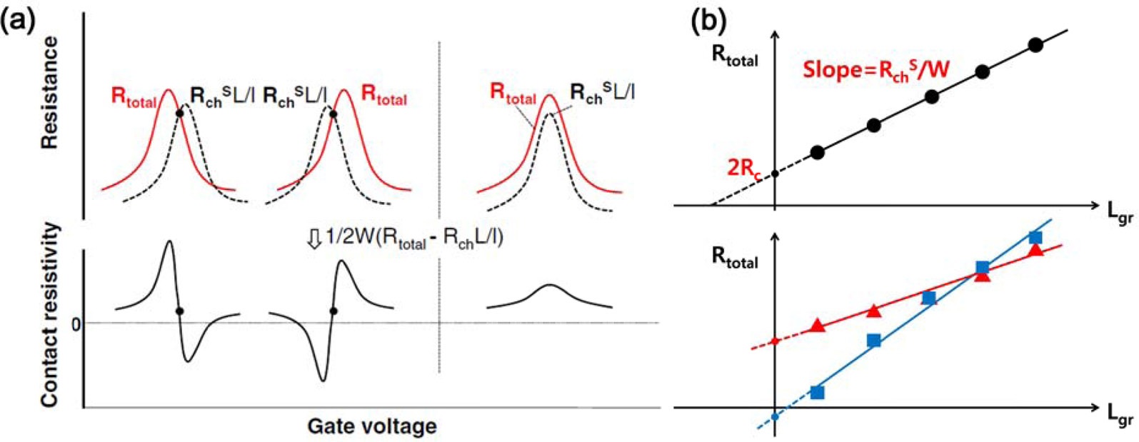
The TLM method is based on the assumption of homogenous properties of the graphene at both the channel and contact regions, such as the Dirac voltage (VDirac), the sheet resistance with respect to the normalized voltage (Vg-VDirac), and the contribution of the metal or the surrounding insulators [43]. These ideal conditions are not possible in the real situations, and errors mostly likely arise. This problem is especially more severe with two terminal devices. The dominant origins of the inhomogeneous properties are the charge puddles in graphene [60,61] and the presence of a charge transfer region due to the metal contact, as explained in the previous section. Charge puddles and/ or chemical doping can be induced by the absorption of ambient molecules or charge transfer from the substrate or residual materials such as the photoresist. Such inhomogeneity can lead to the broadening of the Dirac voltage and result in the suppression of the peak resistance at the Dirac voltage. Many have reported that the contact resistance measured as a function of the gate voltage contains relatively large error bars near the Dirac voltage, as shown in Fig. 4 [21,47]. The charge transfer region induced by the metal contact can play a significant role when the dimensions of the devices are compatible with the carrier mean free path [26]. If doping extends far into the graphene in short channel devices, it can lead to inconsistent sheet resistance in the channel region, provoking errors in measurement. Blake et al. clearly pointed out this issue, reporting that a macroscopic inhomogeneity induced by either chemical doping or metal contacts is an important factor when evaluating the properties of graphene near the Dirac voltage [26]. Fig. 5 illustrates the possible reason behind the errors in the extraction method for the four-point probe method and the TLM method [43]. The inhomogeneous sheet resistance can even lead to negative contact resistance.
There have been many reports on charge puddles or substrateinduced doping [61-65], and it can be suppressed by choosing the optimum dielectric materials or by fabrication devices with well-developed process conditions [66-69]. It has been found that the intrinsic doping of graphene and low hysteresis are obtained by depositing polymers on top of the substrate, such as a hexamethyldisilazane or phenylsilane self-assembled monolayer [24,66]. The utilization of boron-nitride film as a substrate has also been shown to preserve the excellent properties of graphene and significantly suppress the charge inhomogeneity [70-73]. A photoresist layer or chemicals which remain on the graphene during the device fabrication process seriously affect the inhomogeneity of the graphene. To reduce the contamination on the contact region, a plasma treatment prior to metal deposition during the lift-off process has been introduced [74,75].
The low-power plasma in such a process not only removes resist residue on graphene but also creates defects in the contact region of graphene, thereby enhancing the metal-graphene interaction. An O2 plasma treatment process improves the contact resistance by nearly 6000 times compared to a conventional process [74]. It has also been revealed that this technique results in similar levels of contact resistivity regardless of the metal species. In addition to O2, various plasma types such as Ar, N2, and H2 have been exposed to graphene, though O2 plasma has been found to be more effective in making graphene chemically reactive, thereby enhancing the adhesion with the metal [75], It was noted that the metal deposition process also can affect the performance of graphene devices. It has been found that sputtering Ti on graphene greatly degrades the device performance compared to the e-beam evaporation method [76]. Although the sputtering method also generates defects in graphene like the O2 plasma treatment, the situation is somewhat different. Nonetheless, the exact mechanism causing this difference has not been well identified.
At the current stage of graphene technology, the immature process technology is one of the critical obstacles to overcome in order to obtain good contact. The preparation of graphene, the metal deposition process, the substrate condition, or even the measurement environment can all have an impact on the measured contact properties. This can be noticed from the face, where there are widely varied or inconsistent results regarding the contact resistance in previous reports. For example, the Ti contact was predicted to show poor results in one report [25], but in other reports, it results in superior contact properties over other metals [22,57]. The conventional facial contact structure fabricated by the lift-off process is also a limitation when seeking to obtain good contact performance. The transport of carriers in the vertical direction of graphene is known to be different from the nature of the transport on the basal plane. The superior electric properties of graphene are attributed to the π-orbital electrons on the basal plane, while the conduction of the carriers along the c-axis basically originates from the thermal excitation or from impurity-assisted interlayer hopping [77,78]. The carrier transport in the conventional structure with which the metal is deposited on the graphene basal plane is therefore expected to limit how much the performance can be enhanced. To improve the transmission probability of carriers, the dual gate structure which graphene is sandwiched with top and buried metals has been introduced and it results improved contact resistance of 40% compared to the conventional top-contacted structure [79]. Although it is a new approach, the structure also explores the facial contact. An alternative approach to overcome the facial contact is to use the edge contact structure which is formed by a covalent bond between the metal atoms and the graphene; it is expected to show significantly lower contact resistance compared to the facial contact. Theoretical reports estimated that the contact resistivity could be as low as 10 to 103 times the facial contact based on a quantum tunneling process [57]. Very recently, contact modules considering the edge contact resistance were developed [80]. The proposed contact module results in an improvement of approximately 20~60% compared to the conventional method involving a lift-off process.
Graphene-metal contact regions exhibit unique characteristics compared to the conventional semiconductor-metal contact. Graphene can be doped by the contacting metal and the work function strongly depends on the metal species. Work function pinning can form a p-n junction in the graphene channel, leading to asymmetrical conductance behavior and contact resistance. The contact resistance is significantly affected by the density of states of the graphene in the contact and channel regions, engineercausing the gate voltage to modulate the contact resistance. The charge transport at the graphene-metal interface and at the edge of the metal contact determines the intrinsic contact resistance, which must be minimized. Although the exact mechanism has not been suitably explained thus far, the potential profile at the contact edge does not seem to contribute to the contact resistance significantly. As the scattering mean-free path of graphene at the contact point can affect the intrinsic contact resistance, the influence of the substrate can also play a major role in addition to the quality of the graphene. In order to achieve good contact properties, associated process technologies must mature as state-of-the-art CMOS technology. An advanced contact process scheme must also be developed, and the edge contact structure may be a solution in this area.


![(a) Capacitance-voltage (C-Vg) measurement results with various Cr/Au area of metal-oxide-semiconductor capacitor which is illustrated in the inset. (b) The differentiated curves in Fig. 3a clearly show two peaks. (c) The peak heights have strong dependence on the metal area, indicating the presence of two different work functions in graphene underneath the metal and the exposed graphene. (d) The extracted work function of graphene underneath the metal (Φgr/m) and that of the corresponding metals (Φm) (Reprinted with permission from earlier work [47]. Copyright 2012, American Chemical Society).](http://oak.go.kr/repository/journal/12558/HGTSB6_2013_v14n3_162_f003.jpg)
![Extracted contact resistances with the back gate voltage (Rc-Vg) with various metals. The inset shows a microscopic image of a transmission length measurement device (Reprinted with permission from earlier work [47]. Copyright 2012, American Chemical Society).](http://oak.go.kr/repository/journal/12558/HGTSB6_2013_v14n3_162_f004.jpg)
![(a) A possible explanation for the extraction errors from the four?point probe measurement. The contact resistance is obtained from (Rtotal-Rch S·L/l)/2, where Rtotal is the total resistance between the source and drain, Rch S is the channel resistance between the two voltage probes, L is the length between the source and the drain, and l the length between the two voltage probes. When the Dirac voltages are not coincident due to inhomogeneous doping in the channel, negative values or undesired results may arise. Larger error bars near the Dirac voltage normally originate for this reason, but a value at a higher or a lower gate voltage is close to the actual value (Reprinted with permission from earlier research [43]. Copyright 2011, The Japan Society of Applied Physics). (b) In the transmission line model, the inhomogeneous also could lead the extraction errors. Although the data fit in the linear relation in an ideal situation, higher or lower contact resistance can result when the sheet resistances are not consistent with the length between the source and the drain (Lgr), as shown by red-triangle dots or the blue square dots.](http://oak.go.kr/repository/journal/12558/HGTSB6_2013_v14n3_162_f005.jpg)