Graphene [1], a two-dimensional (2D) crystalline monolayer sheet of sp2-bonded carbon atoms arranged in a honeycomb lattice, has attracted great interest after its outstanding electrical [2,3], mechanical [4], and chemical [5] properties were revealed when it was obtained for the first time experimentally in 2004 through mechanical exfoliation (the “scotch tape” method) [6].
Most of the reported methods for synthesizing graphene sheets can be divided into three categories: exfoliation, epitaxial growth, and chemical vapor deposition (CVD). Among the exfoliation methods, besides mechanical exfoliation, chemical exfoliation [7-10] is widely used because it is inexpensive and does not require the transfer of graphene from the growth substrate to other substrates. Furthermore, this method allows for the rapid production of relatively large quantities of graphene. The epitaxial method, which utilizes substrates such as SiC [11] at high temperatures, and the CVD method, which uses CH4 as a gaseous carbon source with nickel [12,13] or copper [14,15] metal as the catalyst substrate, have been used to grow high quality graphene with relatively large areas.
2. Graphene growth from polymers
Recently, CVD has been identified as the most suitable way to obtain graphene with the high transmittance and electrical conductivity of particular interest for electronic devices [12-14,16-20]. However, despite its numerous advantages, the CVD method involves some significant challenges. First, an additional process is required to physically transfer graphene films from the catalyst metal to the receiver substrate. During the transfer process, special care should be taken to avoid degradation of the graphene quality, which in turn may cause performance degradation of the devices in which it is used. Furthermore, the use of explosive hydrocarbon gases as a carbon source, and the limit on film size set by the need to transfer the graphene films after growth, are major obstacles for mass production. Although the use of solid carbon sources for the synthesis of graphene is uncommon, there have been some recent reports of such usage [21-25]. Active research is now in progress to find a promising way to overcome the obstacles of the CVD method. The present review covers the growth of graphene from polymers; using the various solid carbon sources available.
2.1. Polymer-sourced graphene grown on metal film
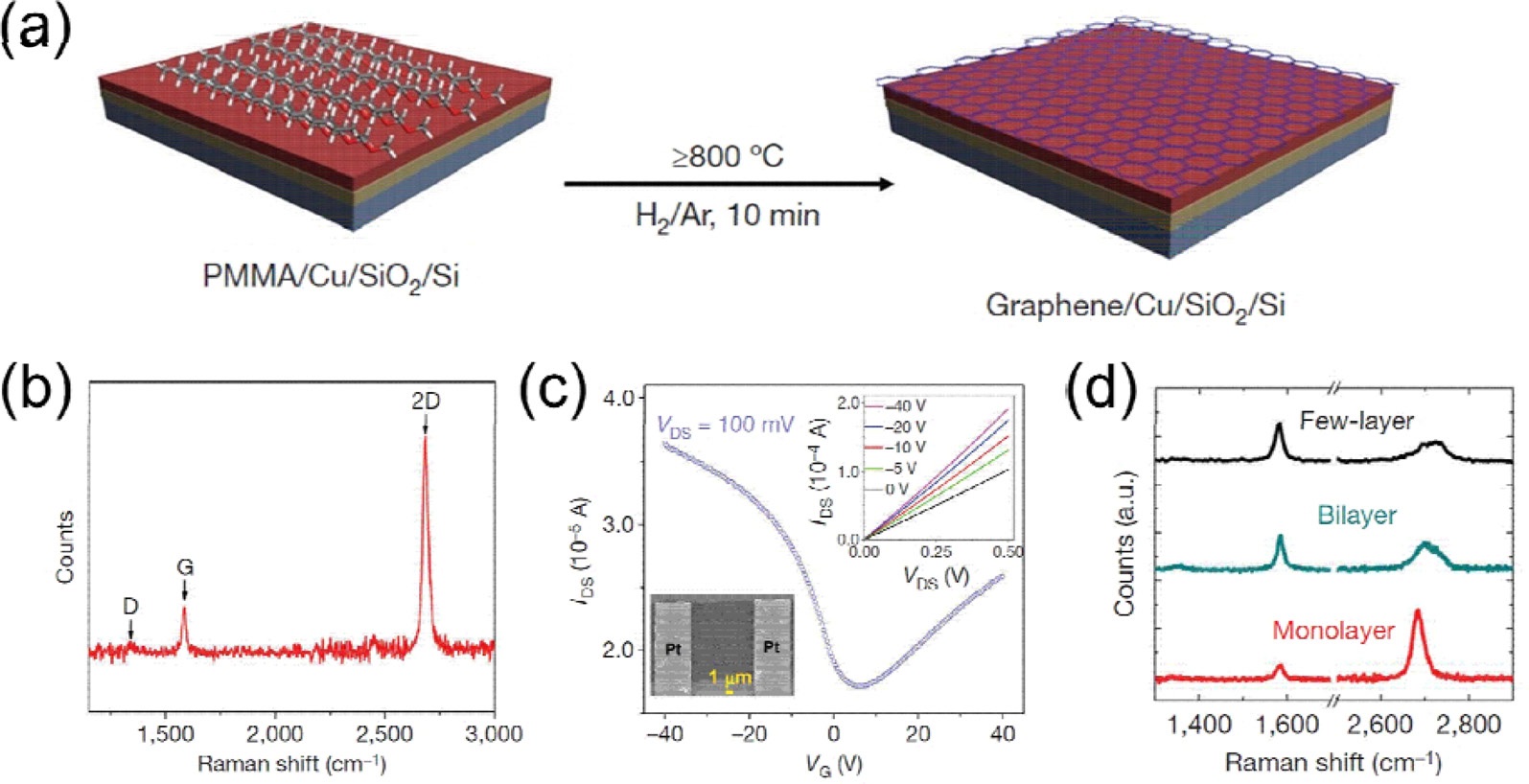
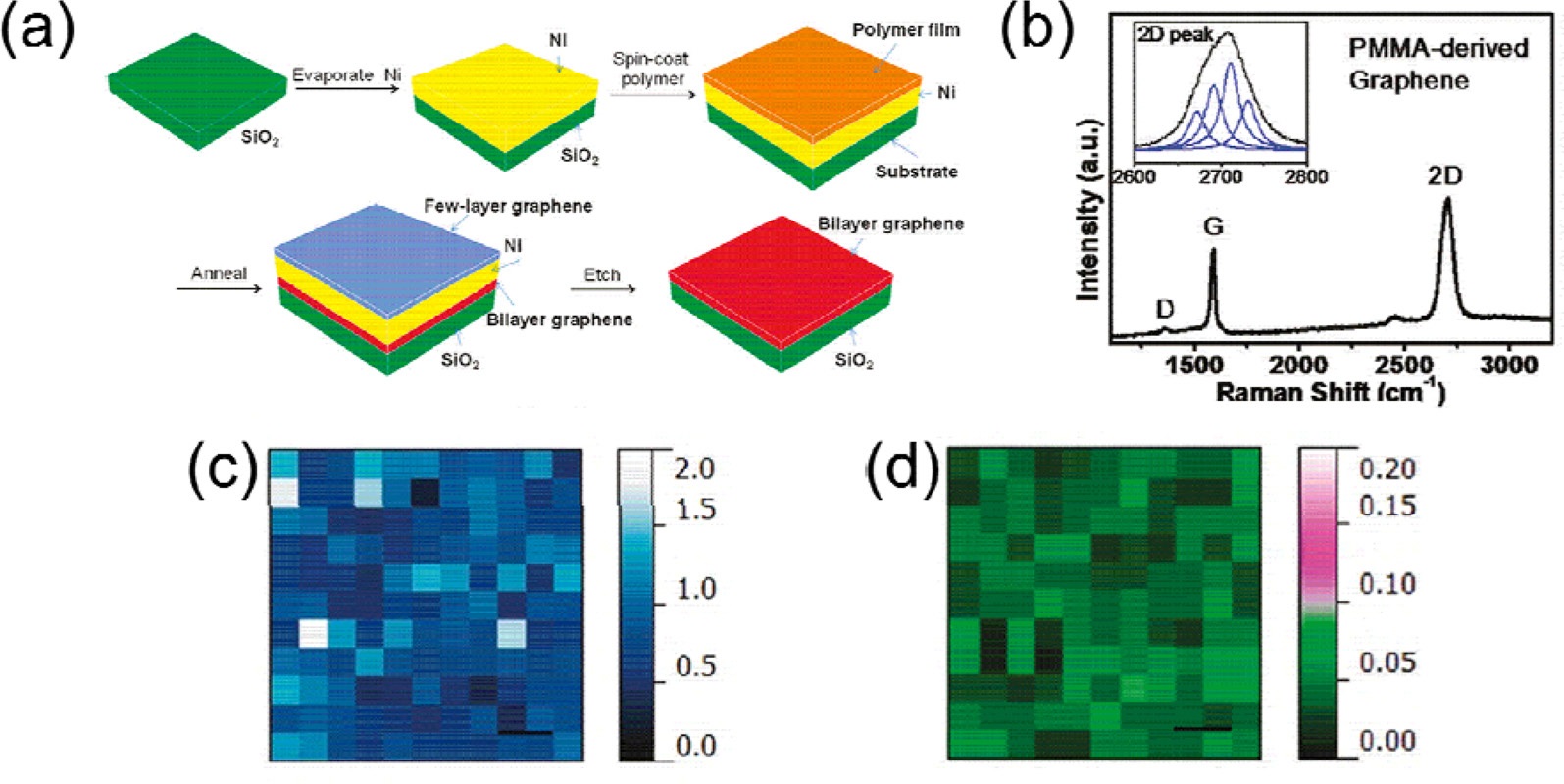
In order to synthesize large-area, high-quality graphene with controllable thickness, Sun et al. [26] used polymer films deposited on metal catalyst substrates. A spin-coated poly(methyl methacrylate) (PMMA) thin film (~100 nm) was used as the first solid carbon source. Copper was used as the metal catalyst substrate for the growth of a graphene-monolayer by surface adsorption, because of its low carbon solubility [14,15,27]. A single uniform layer of graphene was obtained by annealing the samples at temperatures from 800 to 1000℃ for 10 min, under a reductive gas flow (Ar-H2) and low-pressure (Fig. 1a). For further characterization, the graphene films grown were then transferred to various substrates. Fig. 1b shows the Raman spectrum of PMMA-derived graphene, which indicates that it was grown as a monolayer. The electrical properties of the PMMA-derived graphene were evaluated using back-gated (200-nm SiO2 layer), graphene-based, field-effect transistor (FET) devices. The estimated carrier (hole) mobility was ~410 cm2 V-1 s-1 at room temperature, and the “on/off” current ratio was ~2 (Fig. 1c). These researchers found that the thickness of PMMA-derived graphene could be controlled by changing the Ar-H2 gas flow rate (Fig. 1d). These were very significant results because the thickness of graphene is strongly related to its electronic properties [28]. When the H2 flow rate was 3-5, 10, and 50 STP cm3 min-1 or higher; a few layers, a bilayer, and a monolayer of graphene were formed on the Cu substrate, respectively, at 1000℃ under an Ar flow of 500 STP cm3 min-1. They explained that the H2 gas played the role of reducing reagent and carrier to remove carbon atoms from PMMA during growth. A slower H2 flow left more carbon atoms for the formation of thicker layers.
2.2. Polymer-sourced graphene grown directly on insulating substrate
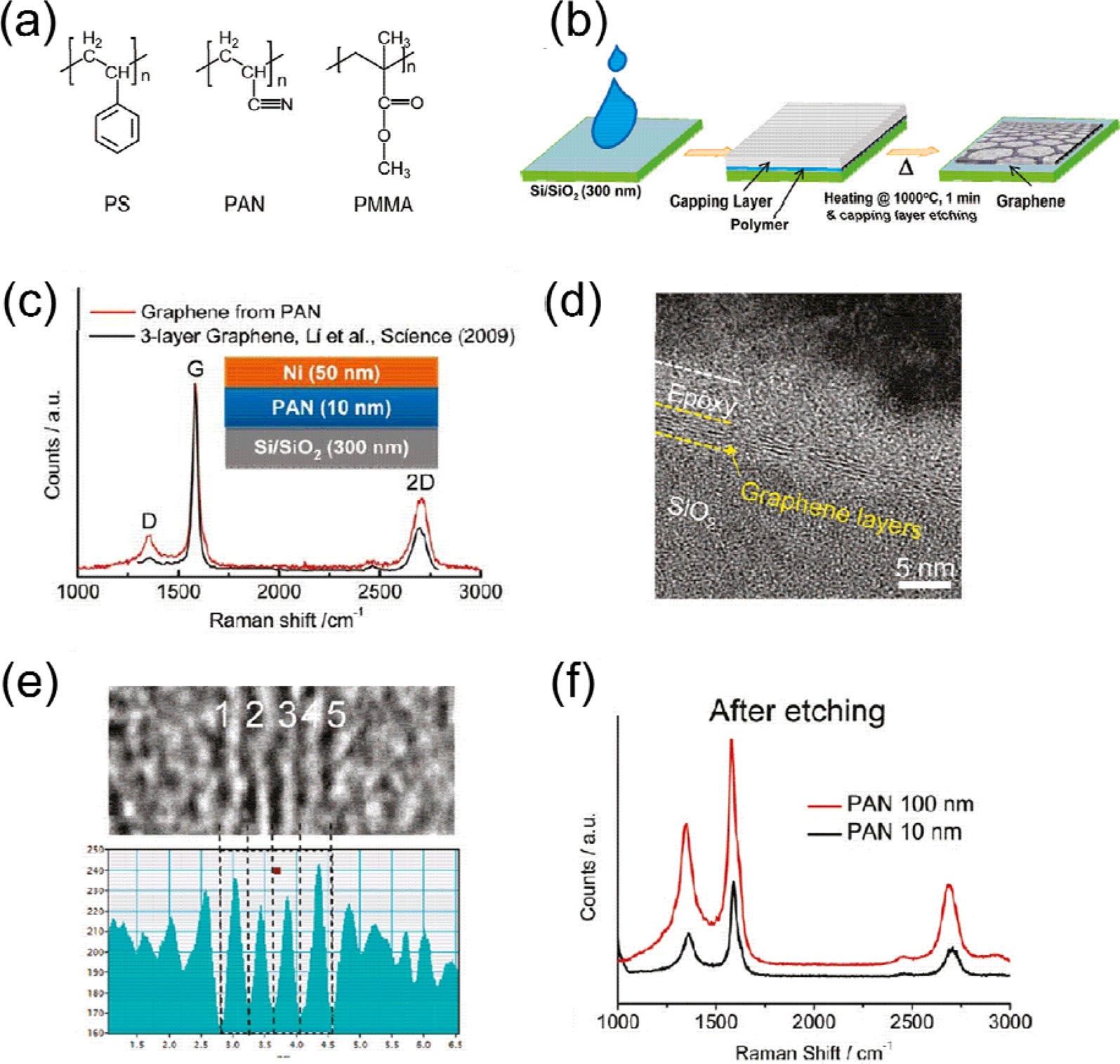
To avoid the physical transfer of the new graphene films from the metal catalyst to other inert substrates, Byun et al. [29] introduced an unprecedented direct growth method that allowed for the synthesis of graphene sheets from common polymers such as polystyrene (PS), polyacrylonitrile (PAN), and PMMA using metal capping layers (Fig. 2a). A film consisting of a few layers of graphene was obtained by capping the polymer films with a Ni layer, and then heating them in a high-temperature furnace, in the presence of by Ar-H2 gas under low vacuum (Fig. 2b). When the polymers were heated to a temperature of 1000℃, above the distinct thermal decomposition temperature
graphene layer underneath the metal surface.
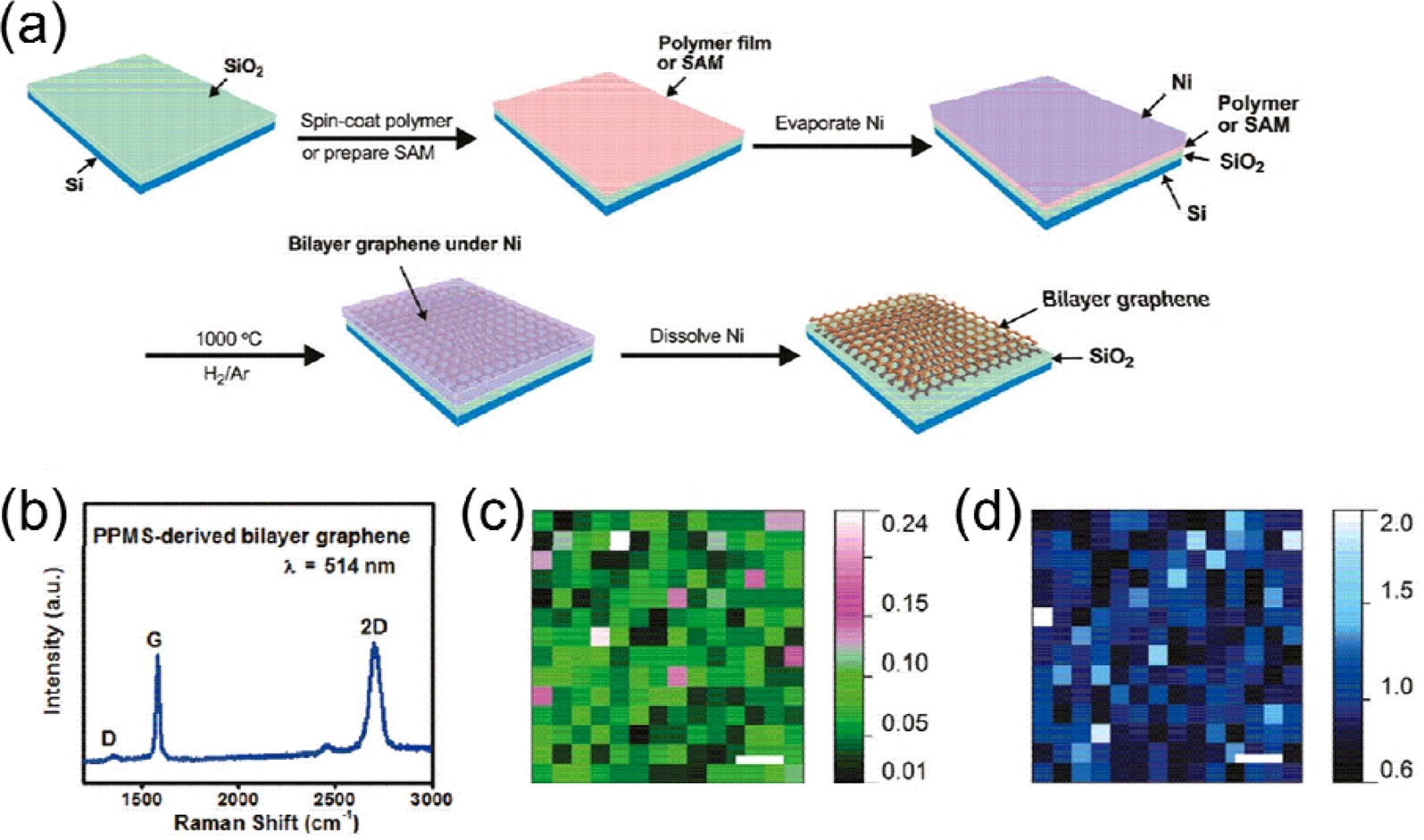
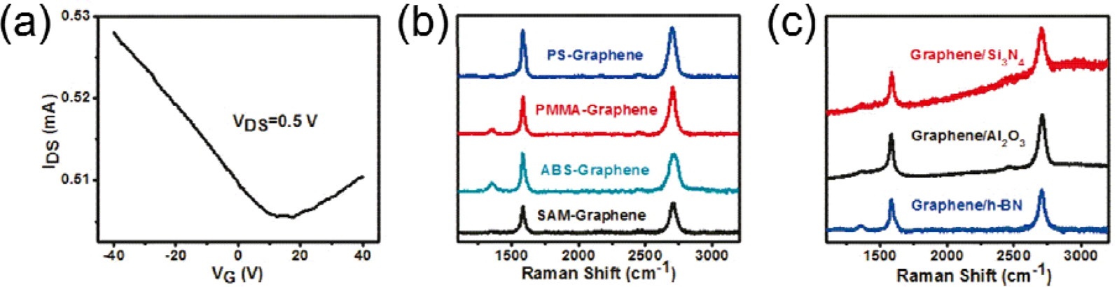
when employing Ni as a catalyst, owing to the continuous supply of carbon and the high solubility of Ni in carbon [12,13]. In this method, the fact that the amount of feed carbon was limited and fixed between the insulating substrate and the Ni film, facilitated the growth of bilayer graphene. Other polymers?PS, PMMA, and ABS?were also converted to bilayer graphene by the direct growth method on insulating substrates; under the same reaction conditions (Fig. 4b). In addition, bilayer graphene was synthesized on several other insulating substrates such as hexagonal boron nitride (h-BN), Si3N4, and Al2O3 (sapphire) (Fig. 4c).
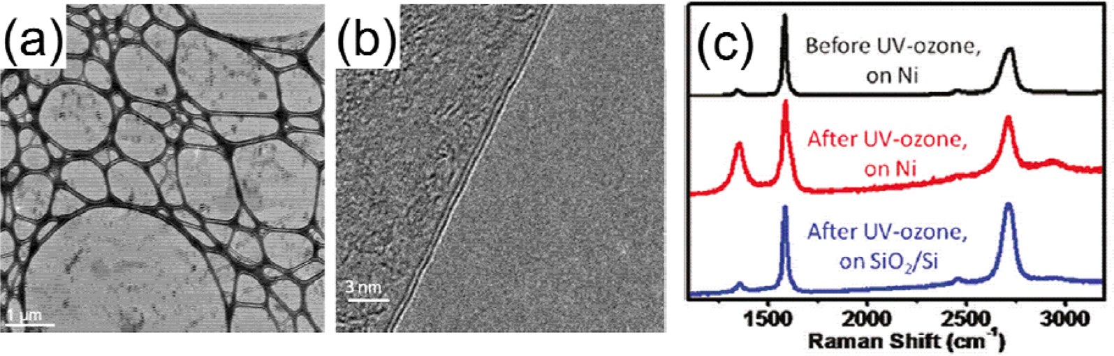
As another approach to direct growth, Peng et al. [40] placed the polymer films on top of the Ni layer. Bilayer graphene was formed between the insulating substrates and the Ni layers as a result of carbon diffusion through the Ni layer at an elevated temperature [41]. Solid polymer films of PMMA, high-impact PS, or ABS were used as carbon sources, and the samples were annealed under Ar-H2 gas flow at 1000℃ for 10 min. The carbon atoms that decomposed from the carbon source diffused into the Ni film at high temperatures and precipitated to form graphene on both sides of the Ni film upon cooling (Fig. 5a). After the Ni layer was removed, bilayer graphene was located directly on the SiO2 substrate. After Ni etching, the Raman spectrum was obtained from the PMMA-derived bilayer graphene on SiO2 (Fig. 5b). The spectrum showed a G peak at 1580 cm-1 and a 2D peak at 2700 cm-1, which were comparable in intensity, and the FWHM of the 2D peak was about 50 cm- 1. The small D peak at 1350 cm-1 indicated that the graphene had few defects. The quality of the PMMA-derived graphene was further confirmed by Raman mapping of the D to G peak intensity ratio. Over ~99% of the map showed a ratio below 0.1 (Fig. 5c), and four-point probe measurement of the graphene film yielded a sheet resistance of about 2000 Ω/sq. The comparable intensities of the G and 2D peaks (Fig. 5b), and the Raman mapping of the G to 2D peak intensity ratio (Fig. 5d), implied that PMMA-derived graphene on SiO2 was bilayered. The PMMA-derived graphene on SiO2 was transferred to a TEM grid and examined using low-resolution TEM (Figs. 6a and b). The results showed two carbon layers, indicating the bilayer characteristic
of the PMMA-derived graphene film. To prove that the graphene films on SiO2 did not originate from the top side of the Ni layer, the surface of the samples was subjected to UV-ozone treatment for 15 min (Fig. 6c). Before the UV-ozone treatment, the graphene film showed a small D peak with
In this review, several graphene synthesis methods using polymers are introduced. In various studies, homogeneous graphene films of large area were obtained. Depending on the film structure, some methods did not require an additional graphene transfer process. These are cost-effective, scalable, and safe ways to grow graphene, and hence are suitable for mass production. When compared with conventional CVD-grown graphene, however, the conductivity of polymer-derived graphene needs to be increased beyond its present value for use in graphene-based electronics. Therefore, further research in this area is necessary to provide a promising way to utilize graphene more practically in the near future.

![(a) Monolayer graphene is made by spin-coating and annealing solid poly(methyl methacrylate) (PMMA) films on Cu substrates at 800 to 1000℃ under an Ar-H2 gas mix; (b) Raman spectrum (514-nm excitation) of PMMA-derived graphene annealed at 1000℃; (c) IDS-VG curve of a PMMA-derived, graphenebased, back-gated field-effect transistor device (at room temperature). The top inset shows the IDS-VDS characteristics; VG changes from 0 V to -40 V. The bottom inset shows a scanning electron microscopy (JEOL-6500 microscope) image of the device in which the PMMA-derived graphene is perpendicular to the Pt leads. (IDS: drain-source current; VG: gate voltage; VDS: drain-source voltage); (d) Raman spectra varied by the number of sheets of PMMA-derived graphene with controllable thicknesses derived from different flow rates of H2 [26] (Reprinted with permission. Copyright 2010, Macmillan Publishers Limited).](http://oak.go.kr/repository/journal/12556/HGTSB6_2013_v14n3_145_f001.jpg)
![(a) Chemical structure of polymers used as graphene precursors; (b) graphene growth process; (c) Raman spectra of PAN-derived graphene film with a 50-nm-thick Ni capping layer annealed at 1000℃ (the capping layer is subsequently removed); (d) cross-sectional high-resolution transmission electron microscopy (HRTEM) image of graphenes formed on a SiO2/Si substrate outside the agglomerated Ni islands; (e) magnified HRTEM image and intensity profile across the graphenes; (f) Raman spectra of PAN-derived graphene with polymer layers of different thickness after removing the capping layer [29] (Reprinted with permission. Copyright 2011, American Chemical Society). PS: polystyrene, PAN: polyacrylonitrile, PMMA: poly(methyl methacrylate).](http://oak.go.kr/repository/journal/12556/HGTSB6_2013_v14n3_145_f002.jpg)
![(a) Bilayer graphene grown directly on a SiO2/Si substrate from a solid polymer or self-assembled monolayer (SAM) film by annealing the sample under an Ar-H2 gas mix at 1000℃ for 15 min; (b) Raman spectrum (514-nm excitation) of PPMS-derived bilayer graphene; two-dimensional (2D) Raman (514 nm) mapping of the bilayer graphene film (112 × 112 μm2): (c) D/G peak ratio; (d) G/2D peak ratio. The color gradient bar is to the right of each map, and the scale bars are equivalent to 20 μm in (c) and (d) [38] (Reprinted with permission. Copyright 2011, American Chemical Society). PPMS: poly(2-phenylpropyl)methylsiloxane.](http://oak.go.kr/repository/journal/12556/HGTSB6_2013_v14n3_145_f003.jpg)
![(a) IDS-VG curve for a PPMS-derived, graphene-based, back-gated field-effect transistor device (room temperature); (b) Raman spectra of graphene converted from polymers (PS, PMMA, ABS) and an self-assembled monolayer (SAM) prepared from butyltriethoxysilane; (c) Raman spectra of graphene derived from PPMS on h-BN, Si3N4, and Al2O3 (sapphire) [38] (Reprinted with permission. Copyright 2011, American Chemical Society). PS: polystyrene, PMMA: poly(methyl methacrylate), ABS: poly(acrylonitrile-co-butadiene-co-styrene), PPMS: poly(2-phenylpropyl)methylsiloxane.](http://oak.go.kr/repository/journal/12556/HGTSB6_2013_v14n3_145_f004.jpg)
![(a) Schematic of the growth of bilayer graphene from polymer films; bilayer graphene is grown directly on a SiO2/Si substrate by spin-coating a polymer film on a Ni layer and annealing the sample under an Ar-H2 gas mix at 1000℃ for 10 min; (b) Raman spectrum of PMMA-derived bilayer graphene; Raman mapping of the PMMA-derived bilayer graphene film (100 × 100 μm2): (c) D/G peak ratio; (d) G/2D peak ratio [40] (Reprinted with permission. Copyright 2011, American Chemical Society). PMMA: poly(methyl methacrylate).](http://oak.go.kr/repository/journal/12556/HGTSB6_2013_v14n3_145_f005.jpg)
![(a) Low-resolution transmission electron microscopy (TEM) image of bilayer graphene films on a TEM grid; (b) high-resolution TEM image of bilayer graphene edges showing two carbon layers; (c) Raman spectra of graphene: from the top of the Ni layer before and after UV-ozone exposure; on the substrate after UV-ozone exposure and removal of the Ni layer [40] (Reprinted with permission. Copyright 2011, American Chemical Society).](http://oak.go.kr/repository/journal/12556/HGTSB6_2013_v14n3_145_f006.jpg)