As the smart electronics get smaller, the basic components of such devices, that is, semiconductors, are required to be smaller and to have multiple functions. Due to the diffraction limit of light, it is not easy to implement a narrow line width of sub wavelength size even with a well patterned mask. The three-dimensional packaging method has been suggested as a novel alternative manufacturing method. High density through-silicon-vias (TSVs) is a major enabler of 3-D integrated circuit (3DIC) technology. Chip stacking using TSVs has been attracting attention because it provides possible performance improvements enabled by the decrease of interconnected delays and total length, as well as allowing the opportunity for heterogeneous integration without compromising form factor [1,2].
For the 3D packaging process, new inspection methods as well as corresponding manufacturing processes should be suggested and demonstrated. One of the important processes is to produce TSVs, which are fine and deep holes used for electrically connecting the stacked wafers vertically. To do this, the depth of the TSVs should be measured and controlled after they are created, because a short hole could lead to an electric disconnection between stacked wafers [3-5]
As TSVs are high-aspect ratio holes, and light cannot reach to the bottom surface of TSVs, it is very difficult to measure their depths precisely using conventional optical metrological methods. On the other hand, scanning electron microscopes or tunneling electron microscopes provide a depth value as well as a profile of the cross section; however, the sections of a wafer desired to be measured in principle should be cut [6]. Some researchers have tried to measure depths of TSVs using infrared (IR) microscopes [7-9] diffraction phenomenon [10] laser interferometry [11,12] and reflectometry[13-14]. However, these methods had practical limitations in terms of measurement resolution, measurement uncertainty, and measurement speed.
In this paper, a low numerical aperture interferometry technique which enables measuring the depth of TSVs is suggested and demonstrated. We assume the limitation of the measurement is caused by the characteristics of the specimens; attenuation of reflection due to structural characteristics of TSVs. A novel interference theory considering the reflection attenuation in the TSVs was proposed and simulated. As a result of simulation, we figured out that the low visibility in interferogram was caused by the unbalanced light intensity between the object and the reference mirror.
Unbalanced light intensity between the object and reference mirror can be balanced by increasing the portion of light that gets into the hole using an aperture stop at the illumination optics. To verify the proposed method, simulation using MATLAB was performed and an experiment using low numerical aperture interferometry was performed. With proposed interferometry, the depths of TSVs could be measured without any damage using a visible white light source. Moreover, the 3-D view can be measured in 5 seconds without destroying samples.
II. REFLECTION ATTENUATION IN HOLE WITH HIGH ASPECT RATIO
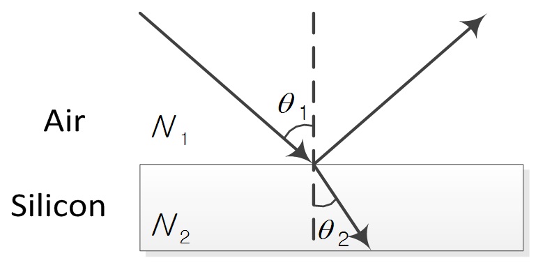
Reflection between two materials can be calculated from complex refractive indices,
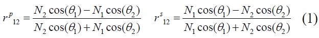
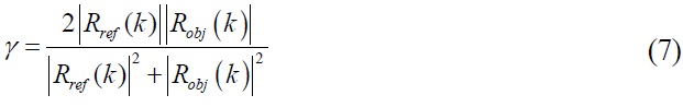
where
propagation angle.
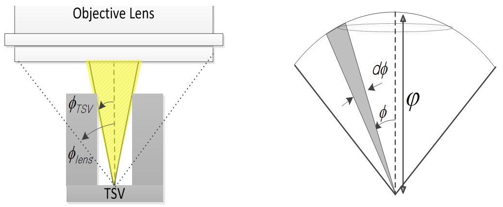
Conventional theories did not take account of the attenuation in light intensity by the structure of the specimen. But in case of TSV measurement with high-power microscopes, not all the incident light reaches to the bottom of the hole as in Fig. 2.
Considering the structural characteristics and the numerical aperture, the reflection from the specimen (TSVs) can be expressed as Eq. (2)
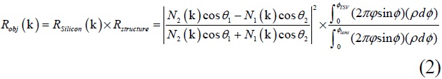
where
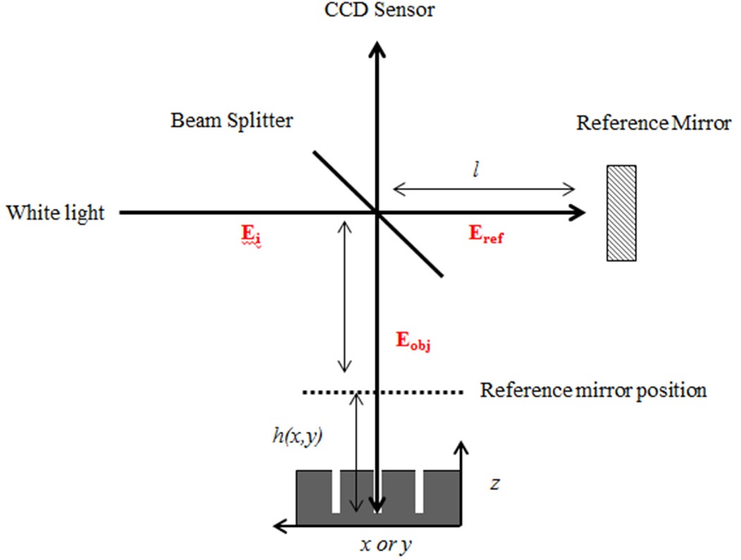
Figure 3 is a basic schematic of the white-light scanning interferometry considered in this investigation, which includes Michelson, Mirau, and Linnik interferometers. The wave equation of the reference light and object light can be expressed as Eq. (3) and Eq. (4)


where,

where,

where,
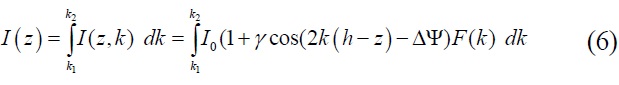
As shown in Eq. (7), unbalanced light intensity causes
decreasing visibility(
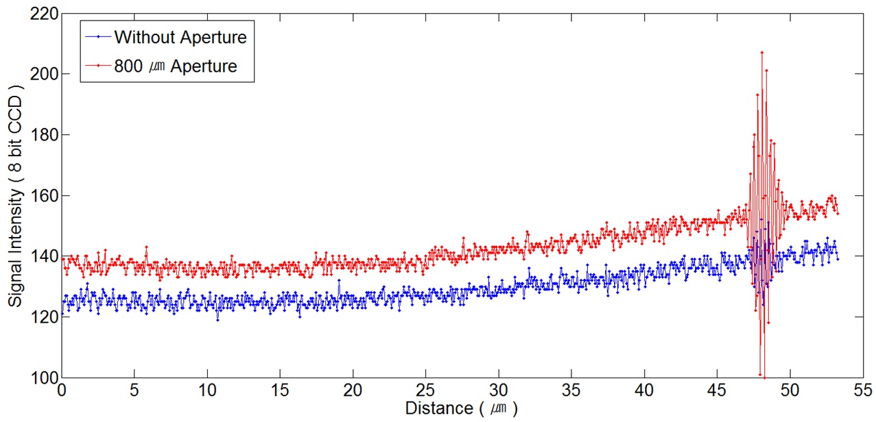
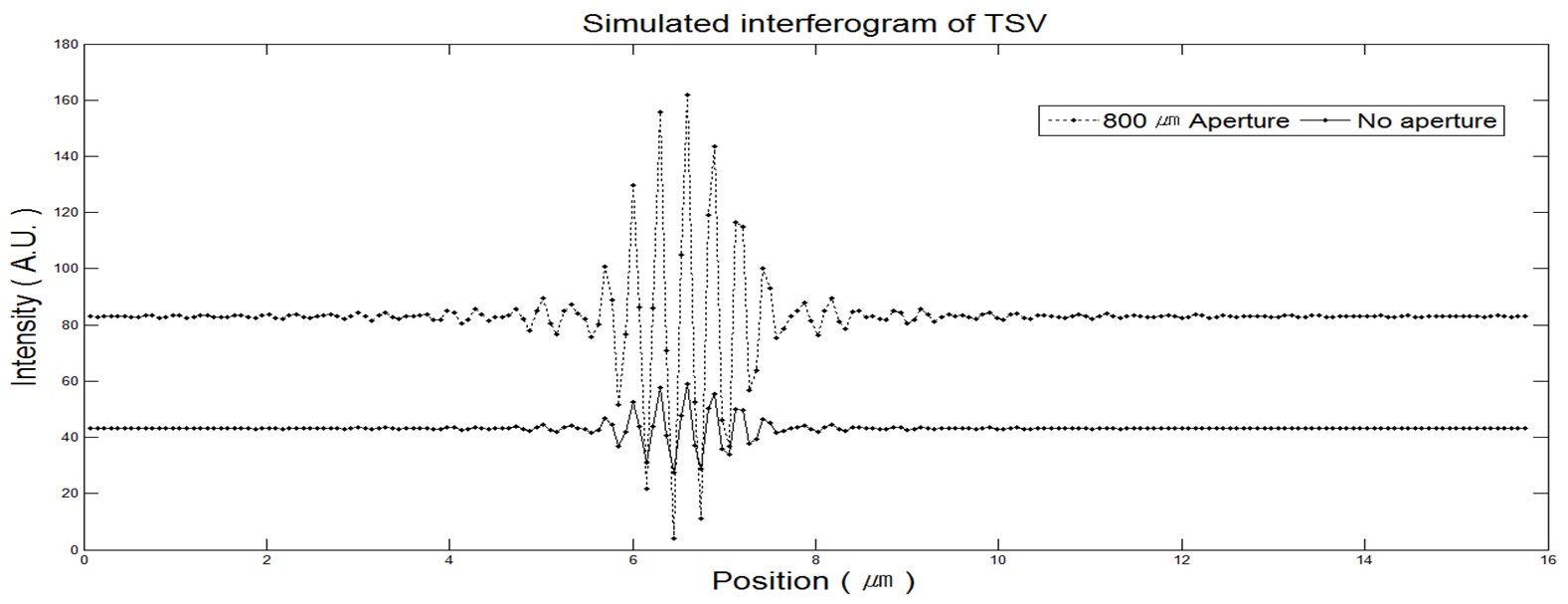
Applying Eq. (2) and Eq. (6), the interference signal can be simulated as Fig. 4, which has an aspect ratio of 11.2 (4.27 ㎛ hole, 47.9 ㎛ depth). The result without an aperture shows low visibility in interference; on the contrary, simulation with the 800 ㎛ aperture shows an enhanced interferogram as dashed line. As a result of simulation, we figured out that the visibility (
III. EXPERIMENTAL SETUP AND DISCUSSION
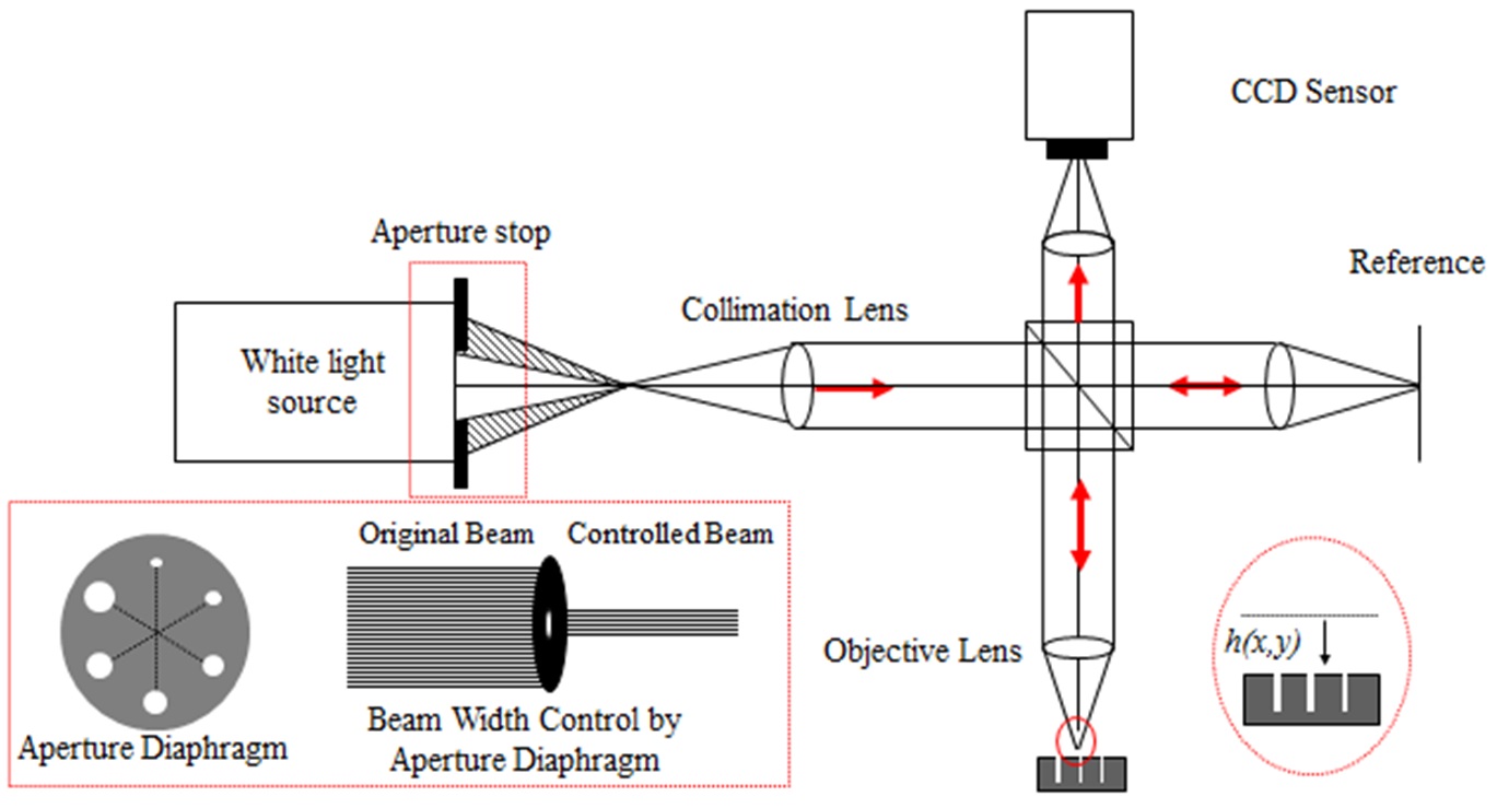
Figure 5 shows the optical layout of the overall measurement system. The aperture positioned at the illumination optics has been set up for implementing a low numerical aperture interferometry. Diaphragm which can mount 6 apertures is instrumented. A Michelson type interferometer was installed with an objective lens having a magnification of 20. The optical path difference between the reference mirror and the surface of the TSVs causes the interference. To scan the sample vertically, a PZT-driven stage having a range of 150 um stroke was exploited.
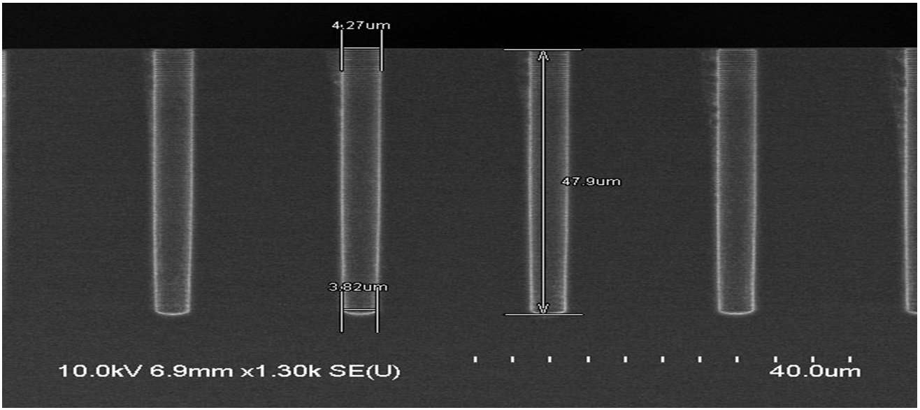
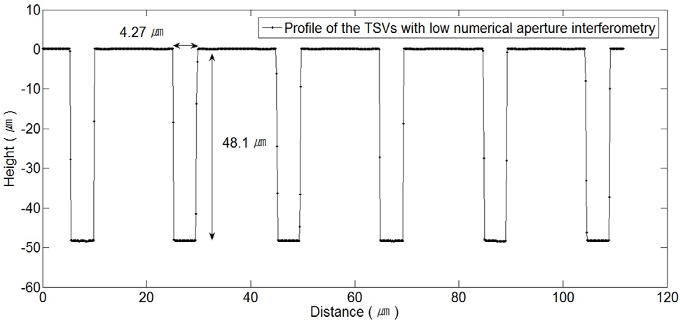
For verification of the proposed method, the sample was fabricated by using a conventional deep-etching process. The sample has many TSVs, as shown in Fig. 6: the diameter and the depth are about 4 ㎛ and ~ 48 ㎛, respectively. To observe the cross-section with SEM, the sample was cut along the axis of TSVs. Fig. 6 shows the SEM measurement result. The diameter of the hole was 4.27 ㎛ and the depth of the hole was 47.9 ㎛.
The interference signal of conventional interferometry and proposed interferometry is shown in Fig. 7. The result without an aperture shows low visibility in interference; on the contrary, interference signal with 800 ㎛ aperture shows an enhanced interference signal as a red line. An interference signal with the aperture can give an enhanced visibility and can give a robust measurement performance. It gives consistent results with the simulation shown in Fig. 3 which expected enhancement of the visibility by applying the aperture stop at the illumination optics.
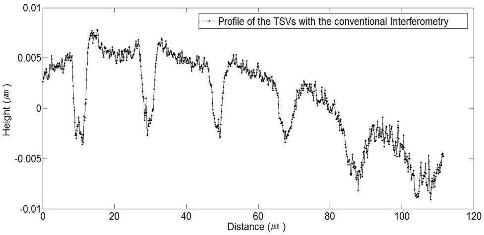
The improved interference signal shown in Fig. 7 enables the measurement of the TSVs. Fig. 8 shows measurement result with the conventional interferometry. The resultant profile cannot represent the actual profile of the TSVs
shown in Fig. 6. Conventional interferometry had failed to measure the bottom of the hole due to high aspect ratio; in contrast, the result with the proposed method is shown in Fig. 9. It shows successful height measurement for both top and bottom of the TSVs a consistent measurement result with the SEM shown in Fig. 6.
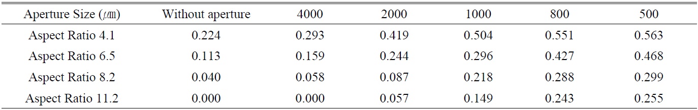
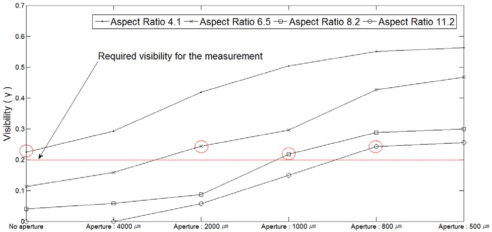
Usually a small aperture creates attenuation in spatial resolution. There exists a tradeoff between spatial resolution and depth measurement. For the optimal condition for both height measurement and spatial resolution, proper aperture depending on the aspect ratio should be selected. Experiments using various apertures were performed and the result is shown in Table 1. Table 1 is drawn in Fig. 10. The largest aperture achieving required visibility (> 0.2) gives the best performance for both height measurement and spatial resolution. Proper aperture depending on the aspect ratio is marked in Fig. 10 with the red line. For example, measurement of the TSVs with an aspect ratio of 4.1 can be measured without aperture because the required visibility can be accomplished without an aperture; on the contrary, for measurement of the TSVs with an aspect ratio of 11.2, the aperture smaller than 800 ㎛ should be instrumented for accomplishing required visibility.
Table 2 shows corresponding result matching between SEM and proposed interferometry. Using proposed optics the depths of the TSVs having aspect ratio ranging from 3.8 to 11.2 were measured successfully (Diameter: 4.27 ㎛ / Depth: 47.9 ㎛). Table 2 shows the comparison of SEM and measured depth value. It shows a consistent measurement
[TABLE 1.] Experimental result of visibility change with respect to the size of aperture stop

Experimental result of visibility change with respect to the size of aperture stop
[TABLE 2.] Measurement result comparison between SEM and interferometry (Depth in ㎛)

Measurement result comparison between SEM and interferometry (Depth in ㎛)
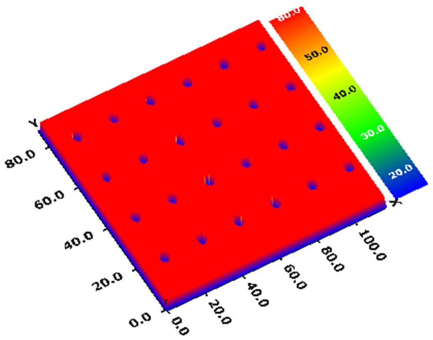
result with the SEM when the aspect ratio is smaller than 11.2. When the aspect ratio is higher than 13, correct measurement result is not guaranteed; it shows the limitation of the proposed method. The limitation occurs when the aspect ratio is higher than 13 because required visibility can no longer be accomplished using proposed optics. 3-D surface measured using the proposed optics is shown in Fig. 11.
The fabrication of TSVs is essential to electrically connect vertically stacked wafers for the 3D semiconductor packaging process. However, the inspection of the TSVs is not an easy task because they have fine and deep holes. Conventional optical methods cannot be used to determine the depth of the TSVs due to the diffraction effect at the edge and stray light in the fine holes. In this paper, for precise depth measurement of the TSVs at high speed, the low numerical aperture technique was proposed and demonstrated.
A novel interference theory which takes the structural reflection attenuation into consideration was proposed and simulated. As a result of simulation, we have come to the conclusion that adopting a proper aperture stop would give an enhanced result for the TSVs. By using a proposed low numerical aperture interferometry, it was possible to obtain the depths and profiles of the TSVs in 5 seconds. With the repeated meadiameter of 4.27surements, the result of the TSVs was a ㎛ and a depth of 47.9 ㎛, and a standard deviation of 0.1 um(3σ). To evaluate the accuracy of the measurement, we made the TSVs samples which have an aspect ratio from 3.75 to 16.9. The measured result showed consistency of 90% between SEM and interferometry data. It is expected that this technique will be used for metrological tools for development of the 3-D semiconductor packaging process as well as in other areas that require the depth measurement of holes with a high aspect ratio.