검색 전체 메뉴
PDF
맨 위로
OA 학술지
Near-infrared Subwavelength Imaging and Focusing Analysis of a Square Lattice Photonic Crystal Made from Partitioned Cylinders
  • 비영리 CC BY-NC
  • 비영리 CC BY-NC
ABSTRACT
Near-infrared Subwavelength Imaging and Focusing Analysis of a Square Lattice Photonic Crystal Made from Partitioned Cylinders
KEYWORD
Photonic crystal , Negative refractive index , Super-lensing , Sub-wavelength imaging
  • I. INTRODUCTION

    In 1968 Veselago proposed that simultaneously negative permeability and permittivity in an isotropic material leads to negative refractive index. According to this fact that the pointing vector and wave vector in these materials are in opposite directions, he called them left-handed materials (LHMs) or negative index materials (NIMs) [1]. As an electromagnetic (EM) wave passes the border between a medium with positive refractive index and a LHM, the beam of light would be refracted to the same side of the normal line as the incident beam. Since no natural material with this specification has been discovered, in the last decade, manufactured structures with effective negative refractive index have attracted a lot of attention due to their wonderful optical properties [2,3] and imaging capabilities [4]. Such meta-materials are able to restore both the phase of propagating waves and amplitude of evanescent waves to make perfect lenses which can overcome the diffraction limit of conventional convex lenses and introduce a new class of imaging systems called “super lenses” [4].

    There are several approaches to realize the negative refraction phenomena. Some meta-materials are made from arrays of metallic split-ring resonators with metallic wire strips. Negative index of refraction in these structures appears in the microwave frequency regime [5-7]. In the optical range of frequency, different designs [8] such as double-plate (or double-wire) pairs, which provide the negative magnetic permeability, and long metal wires [9], are proposed. Another human-made structure is made from arrays of lossless dielectric media named photonic crystals (PCs). These structures are able to explore the effective negative index of refraction in the infrared and optical frequencies. In contrast to the conventional lenses in which imaging effects obey the Newton’s formula, in PCs the imaging is related to mirror-inversion transformation like mirrors although PCs produce real images [10]. Furthermore, there is no need to form a curved surface to obtain an image and also we can attain sub-wavelength imaging which exceeds the diffraction limits [4].

    In these regards, extensive theoretical and experimental imaging studies have been performed [11-14]. Some of the studies on negative refractive index are related to 2D triangular, hexagonal and honeycomb high symmetry lattices in the second band which can be realized as left handed behavior [15-17]. Another kind of research has concentrated on 2D square lattices in which the negative refraction effect occurs in the region of the first photonic band where an isotropic negative index cannot be defined and negative refraction can be conceived by anisotropy or higher-order Bragg scattering effects [18-20]. Focusing properties of 2D square lattice PCs in the second photonic band have been studied experimentally in the range of microwave frequencies [21]. Although negative refraction phenomena in 2D square lattices have been studied extensively, it is of significance to improve efficiency of the superlensing effect especially in near-infrared frequencies.

    In this paper, for evaluation of the negative refraction effect in near-infrared frequency regime in the second photonic band of 2D square lattice PCs, where the wave has a negative phase velocity and PC structure can be assumed as a LHM, we proposed a PC comprising partitioned cylinders. We show that the image position is dependent on the source location and the slab thickness. We employ the finite difference time domain (FDTD) method with periodic boundary condition for calculating the dispersion band diagram of the PC and FDTD method incorporating the perfectly matched layer (PML) boundary condition for simulating the field pattern of the point sources and their images.

    II. BAND STRUCTURE PROPERTIES

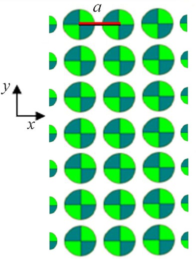
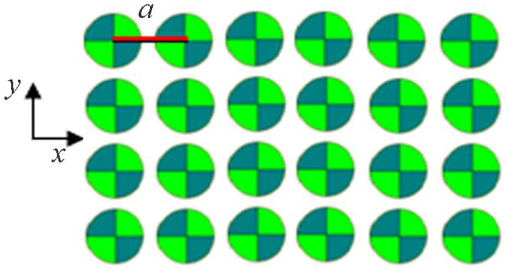
    The PC proposed here is a novel 2D square lattice consisting of periodic arrays of infinitely long dielectric partitioned rods of silica and germanium in air background as depicted in Fig. 1. It is assumed that the width of the slab in the x direction is limited and in the y direction is unrestricted. Dielectric constants of the two substances are εsilica=2.1 and εGe=18 at the wavelength of 1.55 μm and

    the radius of dielectric cylinders is R=0.45a, where a is the lattice constant. We fix the lattice constant at 388 nm which provides the imaging effect at near-infrared frequency regime. According to the configuration of arrays, the TM polarized EM wave is considered for calculating the band structure of the PC and simulating the propagation of the wave in the media.

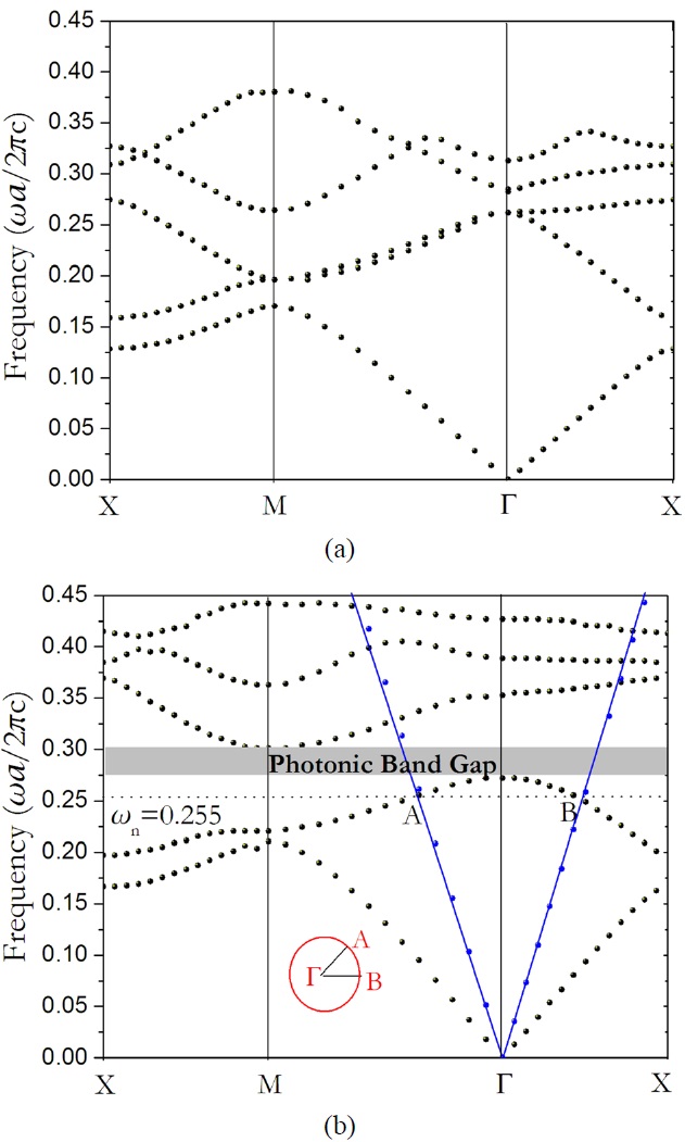
    We employ the FDTD method based on Yee’s lattice to solve the Maxwell’s equations within the unit cell in the time domain by applying the periodic boundary conditions to obtain the band diagram of the PC. We identify the eigenmodes as the spectral peaks from the Fourier transform of the TM mode of the electric field in the time domain. Fig. 2 shows the calculated TM-polarized band diagram along the high-symmetry lines in the first Brillouin zone.

    Fig. 2(a) displays the band diagram of common 2D square lattice PC consisting of Ge cylinders with radius of R=0.45a and Fig. 2(b) depicts the band diagram of partitioned cylinders made from SiO2 and Ge cylinders with the same radii. By comparing these two plots we notice that partitioned cylinders create a complete band gap between second and third bands whereas there is no band gap among the first five bands for TM mode in the already mentioned common square lattice. It should be noted that the first five energy bands of the PC made from SiO2 cylinders, regarding the low dielectric constant of this material, is extended to the frequency of 1.1(2πc/a) and so, it is not suitable for PC superlens application.

    To obtain the frequency with the negative refractive effect we should pay attention to some important conditions. First of all, the frequency should be below 0.5×2πc/a to avoid diffraction and second, the equifrequency surface (EFS) of the PC around the Γ point should have an inward gradient leading to negative group velocity and the last one, the PC’s EFS should contain the EFS of the background [18]. We choose the frequency of the intersection point of PC and air band diagrams to evaluate the imaging properties of this structure. The intersection normalized frequency, ωa/2πc, is around 0.255 and as it is apparent from Fig. 2(b), there is an inward gradient around the Γ point. The

    inset in Fig. 2(b) implies the constant frequency contour with two equal energy surfaces that is related to the second band for ωn=0.255. In fact, the contour approximately looks like a circle and it means that for this frequency the PC can be roughly regarded as an isotropic medium [15].

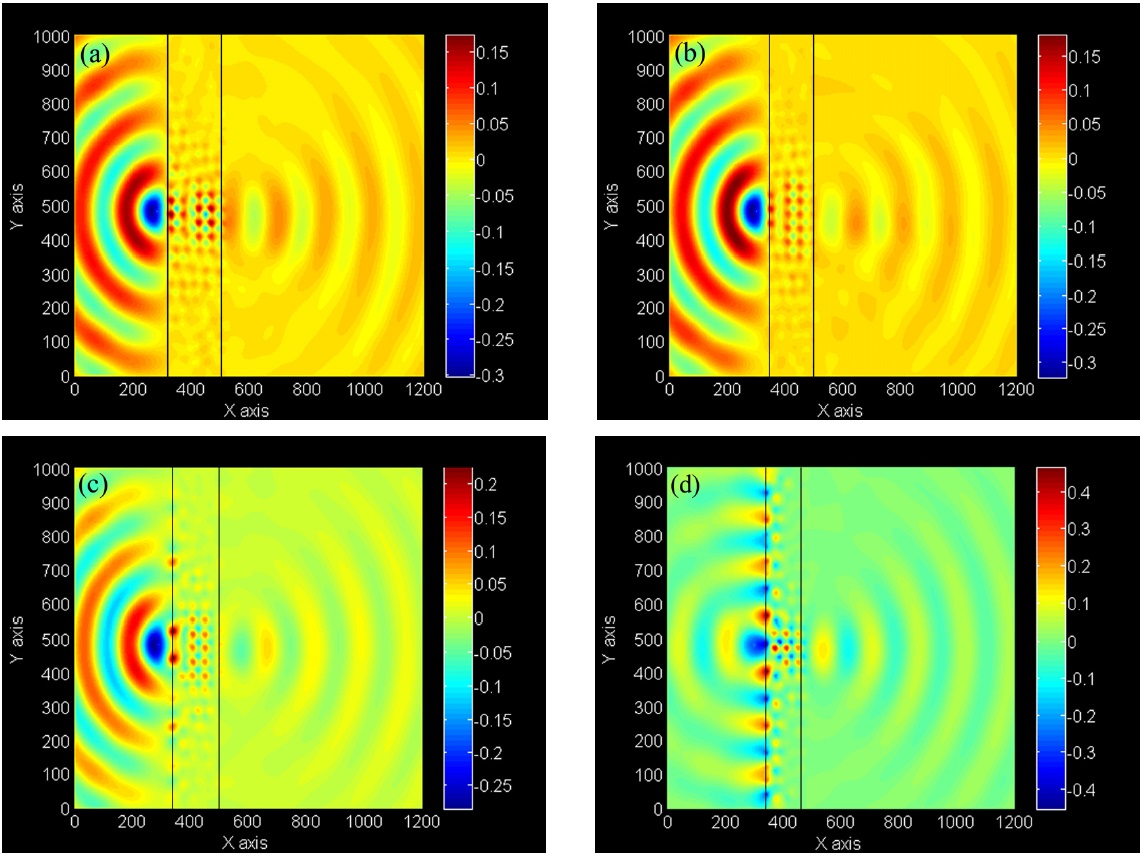
    III. SURFACE TERMINATION EFFECT ON IMAGE QUALITY OF THE PROPOSED STRUCTURE

    There is a type of bound photon mode in photonic crystals that is guided by the background/PC interface. This mode is the linear combination of surface states, those which are strongly affected by the position of surface termination. By coupling incident evanescent waves and bound photon modes, evanescent waves can be transmitted through the PC structure and contribute to image formation [18]. In this regard, some analysis has clarified that surface termination has a significant effect on transmission and image quality [22,23]. According to this issue, we consider a 4.9a-thick slab and put the point source operating at a normalized frequency of 0.255 at distance a from the left side of the PC structure to examine the effect of the air/PC interface on image quality.

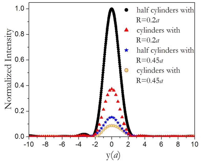
    Figure 3 shows the electric field pattern of the point source and its image when the outmost layers include (a) cylinders with radius R=0.45a, (b) half cylinders with radius R=0.45a, (c) cylinders with radius R=0.2a and (d) half cylinders with radius R=0.2a. It can be inferred that the intensity of transmitted TM-polarized EM wave in the near field region increases with reducing the radius of the outmost cylinders. The surface termination with cylinders of radius 0.2a acts as an anti-reflector to decrease the reflectance. On the other hand, cutting the outmost cylinders leads to participation of the evanescent waves in image formation and improvement of the light intensity at the image site. For the half cylinders with the radius of 0.2a at the interface of air/PC, the evanescent waves are supported and as a result we can find higher resolution and smaller FWHM at the image site. This improvement is also verified by Fig. 4 that transverse distribution of electric field intensity for different surface terminations. By considering this fact, hereafter, we concentrate on the case of PC structures with the preferred surface termination (see Fig. 5).

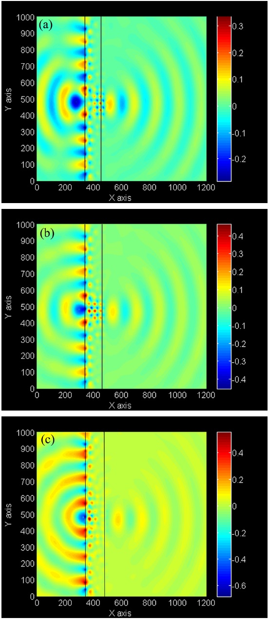
    IV. IMAGE POSITION DEPENDENCY ON THE SLAB THICKNESS AND POINT SOURCE LOCATION

    From the common focusing laws, one can realize whether the designed lens is able to act as a negative index material or not. A number of studies have shown that the overall imaging phenomena in PCs are defined by self-collimating and complex near-field wave scattering effects rather than negative effective index (e.g., see [24]). If the negative refraction mechanism overcomes other phenomena, by increasing the distance of point source from the slab and also by increasing

    the slab thickness, image position should shift to a farther distance. Here, we consider a 4a-thick PC slab to examine the effect of point source location. Fig. 6 shows the electric field pattern outside and beyond the PC structure for this typical slab thickness at normalized frequency of 0.255. In this figure we shift the location of the point source from the far-field to near-field region. In this regard, we put the point source at 1.5a, a and 0.25a from the left side of the slab. When the EM wave is emitted from the point source and enters the slab, the PC focuses the EM wave and forms the image outside the slab. As we expect from the conventional imaging rules, the closer the point source, the farther the image location. By calculating the image position of the point source we realized that by moving the point source from 1.5a to 0.25a, the place of image shifts from 0.5a to 1.9a.

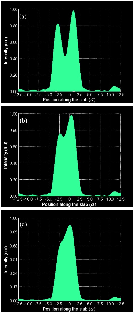
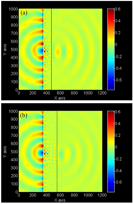
    In Fig. 7 electric field pattern of the point source located at 0.5a from the left side of the PC structure and its image are displayed for different slab thicknesses. We choose 4a and 7a thicknesses for this purpose. As can be seen, by increasing the thickness of the slab, the position of the image shifts from 1.48a to a farther place at 3.05a, as we expect for the NIM slab lenses in which the dominant effect in image formation is negative refraction.

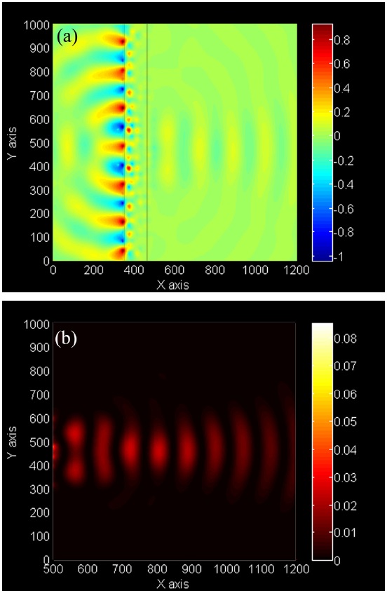
    V. SUBWAVELENGTH IMAGING VIA THE DESIGNED PC LENS

    In order to study the sub-wavelength imaging and evaluate the spatial resolution of the proposed PC lens, we consider two point sources with a given vertical separation distance from each other to observe the peaks of two images clearly and then reduce this distance till the two peaks of images in the right side of the slab become obscure. For this purpose, firstly we put point sources 0.5a away from the PC slab. In this case, they are separated from each other by 3.7a or 0.9435λ in the vertical direction. Fig. 8 shows the electric field distribution and corresponding light intensity when the separation distance of two point sources is 3.7a. From this figure one can recognize two images clearly. Fig. 9 represents the electric field intensity of images in the yz plane for different separation distances. As can be seen, for separation distance of 3.2a, two peaks of images are still clear but when we decrease this distance to 3.1a, only one image can be recognized. Thus, according to Rayleigh criterion [25], for normalized frequency 0.225 and separation distance of 3.2a, the spatial resolution of the system can be regarded as 0.816λ, which is smaller than the incident wavelength.

    VI. CONCLUSIONS

    In this report, we introduced a 2D photonic crystal including partitioned cylinders made from Ge and SiO2 to investigate the image formation characteristics in near-infrared frequency region. We found that despite the usage of the high refractive index material Ge, the band diagram of this structure opens a gap between the second and third bands and satisfies three conditions required to create a PC lens. Although existence of sharp edges in designing such a PC structure makes some difficulties in constructing partitioned cylinders, we showed that this kind of modeling has a potential of PC superlensing in near-infrared frequency with a compressed band structure. In addition, we realized that the image formation depends on the slab thickness and the point source position from the slab. We claim that the imaging effect in our proposed partitioned cylinder PC with a properly terminated surface is dominantly governed by negative refraction effect rather than channeling or near-field scattering effects and according to Rayleigh criterion, the subwavelength focusing can occur with spatial resolution of 0.816λ at the wavelength of 1.55 μm in this structure.

참고문헌
  • 1. Veselago V. G. (1968) “The electromagnetic of substances with simultaneously negative value of ε and μ” [Sov. Phys. Usp.] Vol.10 P.509-514 google cross ref
  • 2. Kim K. Y., Kim S. (2008) “Complete tunneling of light via local barrier modes in a composite barrier with metamaterials” [J. Opt. Soc. Korea] Vol.12 P.314-318 google cross ref
  • 3. Lee C. M., Shim W. S., Moon Y., Seo C. H. (2012) “Design of ultra-wide band-pass filter based on metamaterials applicable to microwave photonics” [J. Opt. Soc. Korea] Vol.16 P.288-291 google cross ref
  • 4. Pendry J. B. (2000) “Negative refraction makes a perfect lens” [Phys. Rev. Lett.] Vol.85 P.3966-3969 google cross ref
  • 5. Zedler M., Caloz C., Russer P. (2007) “A 3-D isotropic left-handed metamaterial based on the rotated transmission-line matrix scheme” [IEEE Trans. Ant. Prop.] Vol.55 P.2930-2941 google
  • 6. Iyer A. K., Eleftheriades G. V. (2008) “Mechanisms of subdiffraction free-space imaging using a transmission-line metamaterial superlens: an experimental verification” [Appl. Phys. Lett.] Vol.92 P.131105 google cross ref
  • 7. Algarin J. M., Freire M. J., Lopez M. A., Lapine M., Jakob P. M., Behr V. C., Marques R. (2011) “Analysis of the resolution of split-ring metamaterial lenses with application in parallel magnetic resonance imaging” [Appl. Phys. Lett.] Vol.98 P.014105 google cross ref
  • 8. Shalaev V. M. (2007) “Optical negative index metamaterials” [Nature Photonics] Vol.1 P.41-48 google cross ref
  • 9. Dolling G., Enkrich C., Wegener M., Soukoulis C. M., Linden S. (2006) “Simultaneous negative phase and group velocity of light in a metamaterial” [Science] Vol.312 P.892-894 google cross ref
  • 10. Notomy M. (2000) “Theory of light propagation in strongly modulated photonic crystals: refraction-like behavior in the vicinity of the photonic band gap” [Phys. Rev. B] Vol.62 P.10696-10705 google cross ref
  • 11. Sukhovich A., Merheb B., Muralidharan K., Vasseur J. O., Pennec Y., Deymier P. A., Page J. H. (2009) “Experimental and theoretical evidence for subwavelength imaging in photonic crystals” [Phys. Rev. Lett.] Vol.102 P.154301 google cross ref
  • 12. Cui Y., Liu K., Foland S., Choi K. H., Tinker M., Farlane D. M., Lee J. B. (2010) “Silicon-based thermo-optically tunable photonic crystal lens” [IEEE Photon. Tech. Lett.] Vol.22 P.21-23 google cross ref
  • 13. Cui Y., Tamma V. A., Lee J., Park W. (2010) “Mechanically tunable negative-index photonic crystal lens” [IEEE Photon. J.] Vol.2 P.1003-1012 google cross ref
  • 14. Hofman M., Lippens D., Vanbesien O. (2010) “Image reconstruction using a photonic crystal based flat lens operating at 1.55 μm” [Appl. Opt.] Vol.49 P.5806-5813 google cross ref
  • 15. Wang X., Ren Z. F., Kempa K. (2004) “Unrestricted superlensing in a triangular two dimensional photonic crystal” [Opt. Express] Vol.12 P.2919-2924 google cross ref
  • 16. Li J., Lu M. H., Fan T., Liu X. K., Feng L., Tang Y. F., Chen Y. F. (2007) “All-angle negative refraction imaging effect with complex two-dimensional hexagonal photonic crystals” [J. Appl. Phys.] Vol.102 P.073538 google cross ref
  • 17. Lin K. M., Guo G. Y. (2008) “Uncoupled modes and all-angle negative refraction in walled honeycomb photonic crystals” [J. Opt. Soc. Am. B] Vol.25 P.C75 google cross ref
  • 18. Luo C., Johnson S. G., Joannopoulos J. D., Pendry J. B. (2003) “Subwavelength imaging in photonic crystals” [Phys. Rev. B] Vol.68 P.045115 google cross ref
  • 19. Huang Y. J., Lu W. T., Sridhar S. (2007) “Alternative approach to all-angle negative refraction in two-dimensional photonic crystals” [Phys. Rev. A] Vol.76 P.013824 google cross ref
  • 20. Tang Z., Peng R., Ye Y., Zhao C., Fan D., Zhang H., Wen S. (2007) “Optical properties of a square-lattice photonic crystal within the partial band gap” [J. Opt. Soc. Am. A] Vol.24 P.379-384 google cross ref
  • 21. Parimi P. V., Lu W. T., Vodo P., Sridhar S. (2003) “Photonic crystals: imaging by flat lens using negative refraction” [Nature] Vol.426 P.404 google cross ref
  • 22. Li Z. Y., Lin L. L. (2003) “Evaluation of lensing in photonic crystal slabs exhibiting negative refraction” [Phys. Rev. B] Vol.68 P.245110 google cross ref
  • 23. Wang H. W., Wu M. L., Chen L. W. (2010) “Focusing analysis of a complex photonic crystal slab with negative refraction” [Physica B] Vol.405 P.4157-4162 google cross ref
  • 24. Xiao S., Qiu M., Ruan Z., He S. (2004) “Influence of the surface termination to the point imaging by a photonic crystal slab with negative refraction” [Appl. Phys. Lett.] Vol.85 P.4269-4271 google cross ref
  • 25. Xia F., Yun M., Liu M., liang J., Kong W., Tan H., Lv W. (2013) “Negative refraction subwavelength imaging in a hexagonal two-dimensional annular photonic crystal” [J. Appl. Phys.] Vol.113 P.013109 google cross ref
OAK XML 통계
이미지 / 테이블
  • [ FIG. 1. ]  2D square lattice PC embracing partitioned cylinders with lattice constant a. Darker parts of cylinders indicate SiO2 and the bright parts represent Ge.
    2D square lattice PC embracing partitioned cylinders with lattice constant a. Darker parts of cylinders indicate SiO2 and the bright parts represent Ge.
  • [ FIG. 2. ]  Photonic band structure of (a) the common square lattice PC consisting of Ge cylinders in air with radius R=0.45a, and (b) corresponding structure composed of partitioned Ge and SiO2 cylinders with the same radius. The lines originated from Γ point depict the light lines in vacuum. Inset: the constant frequency counter of second band related to A and B points.
    Photonic band structure of (a) the common square lattice PC consisting of Ge cylinders in air with radius R=0.45a, and (b) corresponding structure composed of partitioned Ge and SiO2 cylinders with the same radius. The lines originated from Γ point depict the light lines in vacuum. Inset: the constant frequency counter of second band related to A and B points.
  • [ FIG. 3. ]  Electric field distribution of a point source located at the distance a from the left of the PC slab and at normalized frequency of 0.255 when the interface layer at both sides of the slab consists of (a) cylinders with radius R = 0.45a, (b) half cylinders with R = 0.45a, (c) cylinders with R = 0.2a and (d) half cylinders with R = 0.2a.
    Electric field distribution of a point source located at the distance a from the left of the PC slab and at normalized frequency of 0.255 when the interface layer at both sides of the slab consists of (a) cylinders with radius R = 0.45a, (b) half cylinders with R = 0.45a, (c) cylinders with R = 0.2a and (d) half cylinders with R = 0.2a.
  • [ FIG. 4. ]  Transverse distribution of the electric field intensity at the focusing place for different surface terminations at the normalized frequency of 0.255.
    Transverse distribution of the electric field intensity at the focusing place for different surface terminations at the normalized frequency of 0.255.
  • [ FIG. 5. ]  2D square lattice PC consisting of partitioned cylinders with optimum surface termination. The radius of the half cylinders at the interface of air/PC is 0.2a.
    2D square lattice PC consisting of partitioned cylinders with optimum surface termination. The radius of the half cylinders at the interface of air/PC is 0.2a.
  • [ FIG. 6. ]  Electric field distribution of a point source located at (a) 1.5a, (b) a and (c) 0.25a from the left side of the 4a-thick PC slab for normalized frequency of 0.255.
    Electric field distribution of a point source located at (a) 1.5a, (b) a and (c) 0.25a from the left side of the 4a-thick PC slab for normalized frequency of 0.255.
  • [ FIG. 7. ]  Electric field distribution of a point source operating at normalized frequency of 0.255 and located at 0.5a from the left side of (a) the 4a and (b) the 6a-thick PC slabs.
    Electric field distribution of a point source operating at normalized frequency of 0.255 and located at 0.5a from the left side of (a) the 4a and (b) the 6a-thick PC slabs.
  • [ FIG. 8. ]  (a) Electric field distribution of two point sources located at 0.5a from the left side of the PC slab and with 3.7a separation distance between them. (b) Corresponding electric field intensity of images on the right side of the PC slab.
    (a) Electric field distribution of two point sources located at 0.5a from the left side of the PC slab and with 3.7a separation distance between them. (b) Corresponding electric field intensity of images on the right side of the PC slab.
  • [ FIG. 9. ]  (a) Electric field intensity related to images of two point sources which are separated vertically by a distance of (a) 3.7a, (b) 3.2a, and (c) 3.1a.
    (a) Electric field intensity related to images of two point sources which are separated vertically by a distance of (a) 3.7a, (b) 3.2a, and (c) 3.1a.
(우)06579 서울시 서초구 반포대로 201(반포동)
Tel. 02-537-6389 | Fax. 02-590-0571 | 문의 : oak2014@korea.kr
Copyright(c) National Library of Korea. All rights reserved.