Modern personal communication electronics demand the integration of analog, digital, and radio frequency (RF) circuits on a chip. It is common to find these integrated circuits (ICs) inside cell phones, laptops, tablets, and personal computers (PCs). It is important to embed RF circuits not only for improved fabrication quality control but also for tuning of the RF circuit elements to fit multistandard wireless communication platforms. The essential embedded RF test circuits introduced in this paper are the RF power detectors, RF power control circuits, directional couplers, and six-port reflectometers (SPRs). The embedded RF test circuits are generally simple and compact. The conventional approaches and our new approach for these important embedded RF test and RF tuning circuits are introduced in this paper.
RF power detectors are the primary test elements in embedded RF testing systems. The RF power detectors convert input RF power signals to representative DC voltages. The power detectors can be implemented as peak detectors (envelop detectors) or root-mean-square (RMS) detectors [1,2]. The peak detector operations can be understood simply as a combination of a diode and a capacitor. The input RF signals are tailored by the diode. Then, the capacitor stores the peak value of the charge. Depending on the circuit design techniques, the DC levels can be measured as peak or RMS values. RMS RF power detectors may be found to be more useful than peak detectors in many wireless applications. However, generally, RMS detectors are more complex and require a larger chip area. RMS power detectors can be implemented using thermal detection, diode detection, or translinear detection methods [3]. Thermal-based RF power detectors convert the input RF power to the thermal power and measure the ambient temperature changes [4]. The detectors can achieve wide bandwidth and good accuracy. However, the detectors may not be a good candidate for embedded testing because of the thermal coupling from the adjacent circuits. Diode detectors can be implemented as RF RMS detectors by exploiting their square-law characteristic in a small signal operation region [5]. However, the circuits require Schottky diodes, which are not available in a standard CMOS process. Translinear RF detectors have V-I conversion and squarerdivider circuits. Previous research demonstrated that reasonably sized translinear RF detectors are suitable for embedded RF testing [6]. However, translinear circuits can have a limited frequency response below 1 GHz.
III. RF POWER CONTROL CIRCUITS
Input and output RF power may be attenuated or amplified in many wireless applications. One power control method is to build automatic gain control (AGC) systems. These AGC systems can achieve RF power control with fine gain steps and good dynamic ranges [7,8]. However, they tend to require a large chip area. Large area circuits are poor candidates for embedded RF testing.
Variable gain amplifiers (VGAs) are parts of the AGC and, they can be used as a single element to control RF power as an open-loop system [9]. Where the type of gain control input for a VGA is digital, the circuit is called a digital variable gain amplifier (DVGA) [10]. In certain wireless applications, it is important to make the gain control circuits broadband. One of the methods is to utilize distributed amplifiers [11].
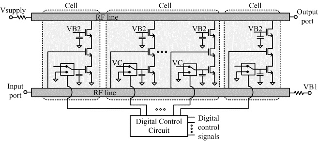
We have developed a mixed system with distributed amplifiers and digital gain control circuits resulting in broadband, digital, and fine gain control steps. A block diagram of the programmable gain distributed amplifier (PGDA) is shown in Fig. 1. Two RF lines are utilized, and the circuit has three cells, where each cell has one or more digitally controllable amplifiers. The middle cell has multiple amplifiers, and the cell can generate various digitally controlled transconductances. One of the published PGDAs is the CMOS PGDA with 0.5 dB gain steps [12].
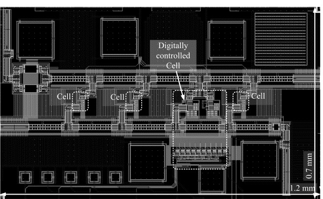
It is designed, fabricated, and measured successfully using a 130 nm process consisting of four cells, where each cell includes an amplifier block.
The amplifier block in the 3rd cell contains multiple amplifiers, where the amplifiers are controlled digitally by the digital control circuit block. The input signals for the digital control block are 3 bit digital signals and a clock signal. The control signals generated by the digital control block make each amplifier active or inactive. Then, the total transconductance gets varied digitally because it is equal to the summation of all the transconductance of the cells. The core layout of the chip using a Cadence IC design tool is shown by a screenshot in Fig. 2. The core chip area is 1.2 mm × 0.7 mm. The area of the chip can be reduced, by 33% of the vertical and 80% of the horizontal length of Fig. 2.
The directional couplers are the core elements for reflection of the measurement circuits. They are generally fabricated as coupled microwave lines. However, in low frequency applications, these coupled microwave lines take too large a chip area for embedded test circuits.
Therefore, lumped directional couplers may be a better choice because they take less chip area for low frequency applications [13,14]. Moreover, by making the directional couplers tunable, they become more flexible and fit many wireless standards [15]. It is a challenge to design tunable directional couplers that are both broadband and highly reconfigurable.
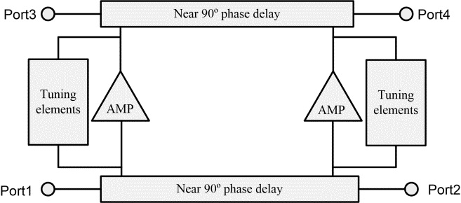
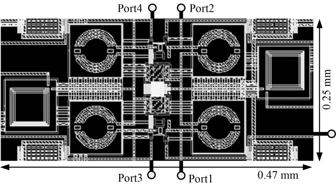
The authors have developed tunable broadband active directional couplers that are suitable for embedded RF testing to satisfy both needs of being broadband and highly reconfigurable [16]. A simplified generalized block diagram of the tunable active directional coupler is described in Fig. 3. There are two amplifiers and tuning elements connected between two near 90° phase delays. The near 90° phase delay represents the RF elements and introduces a phase shift of approximately 90°. Circuit parasitics and variable capacitors from the tuning elements will change the degree of the phase delay between the RF lines while the coupler circuit is tuned. If one applies the input signals at port 1, port 2 is a through port with 90° phase shifted signals from the input signals. Port 4 is a constructive port combining the signals from port 1 and port 2. However, port 3 is a deconstructive port cancelling out the signals from port 2. The detailed theoretical background of this type of directional coupler can be found in [16], where it shows the specific design, fabrication, and measurement of a tunable active directional coupler circuit with 2.4 GHz bandwidth broadband. The core layout of the chip, a screenshot using the Cadence IC design tool, is shown in Fig. 4, where the area is 0.47 mm × 0.25 mm. The phase shifters are implemented as two inductors and capacitors. One of the phase shifters is located in between port 1 and port 2, and the other phase shifter is between port 3 and port 4. There are also two more small size on-chip bias inductors found in Fig. 4.
>
A. Reflectometer for Embedded RF Testing
Vector network analyzers (VNAs) are widely used to measure reflection coefficients and gain. The VNAs include RF power detectors, a power control system, directional couplers, and other types of RF circuits. However, conventional VNAs have fairly complicated hardware and software, and they may consume a large amount of chip space, which makes them unsuitable for the embedded RF test. Reflectometers are devices that can measure signal reflections. One of the candidates for reflectometers suitable for embedded RF testing is a SPR. The primary advantages is that SPRs have is a simple circuit structure. However, the calibration method of SPRs is more complicated than conventional VNA error correction.
>
B. Theory and Calibration of the SPR
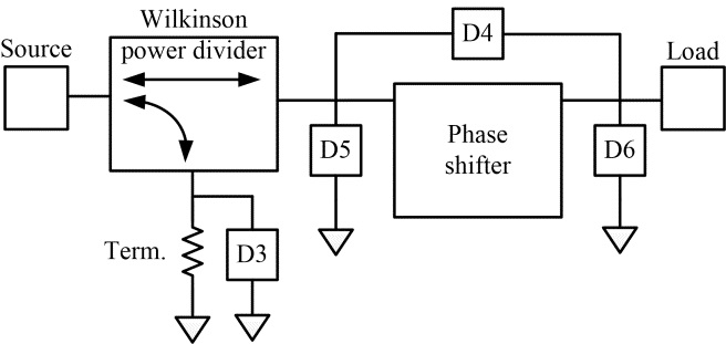
The SPR was popularized by Engen [17,18] and others. One published SPR on-a-chip can work from 1.3 to 3.0 GHz [19]. The authors have developed on-chip SPR systems at high frequencies. The block diagram of a 77-GHz SPR is shown in Fig. 5. It has one divider, one phase shifter, three single ended RF power detectors (D3, D5, and D6), and one differential RF power detector (D4). The details of the single-ended and differential RF detectors can be found in Widemann and colleagues’ paper [19]. And, their SPR calibration method was adopted [20]. The SPR calibration takes the following steps. First, the detectors are characterized properly by changing the input power levels. This method of in situ detector characterization is essential, where the in situ detector characterization means that the detectors are characterized without disconnecting them from the circuit [21]. Next, initial values are estimated for the calibration constants. There are various methods of finding these initial values in the literature [22-24]. The method in this research use a minimum of five unknown loads with constant magnitude reflection coefficients and well-distributed phases [20].
The next step is to perform a six- to four-reductions to decrease the number of the required coefficients of the SPR. A SPR requires eleven coefficients; however, a four-port reflectometer requires six coefficients. Engen presents an approach to perform calibration in a reduced four-port reflectometer [22].
The next step is to carry out an “error box” transformation, which is a mapping technique for the reflection coefficient from the W plane to the Γ plane. The important variables of an SPR calibration, a, b, and c, can be found using three known loads and by solving three linear equations. There are also other calibration methods reported in the literature [25,26].
>
C. 77-GHz SPR Design, Simulation, and Verification
The spectrum range of the W-band is from 75 to 110 GHz. A frequency of around 77 GHz is generally utilized for automotive radar system applications. This section presents an on-chip SPR targeted at 77 GHz. The circuit is designed using a 130 nm process, as shown in Fig. 5. For the power divider, a microstrip Wilkinson power divider was chosen and designed to work at 77 GHz.
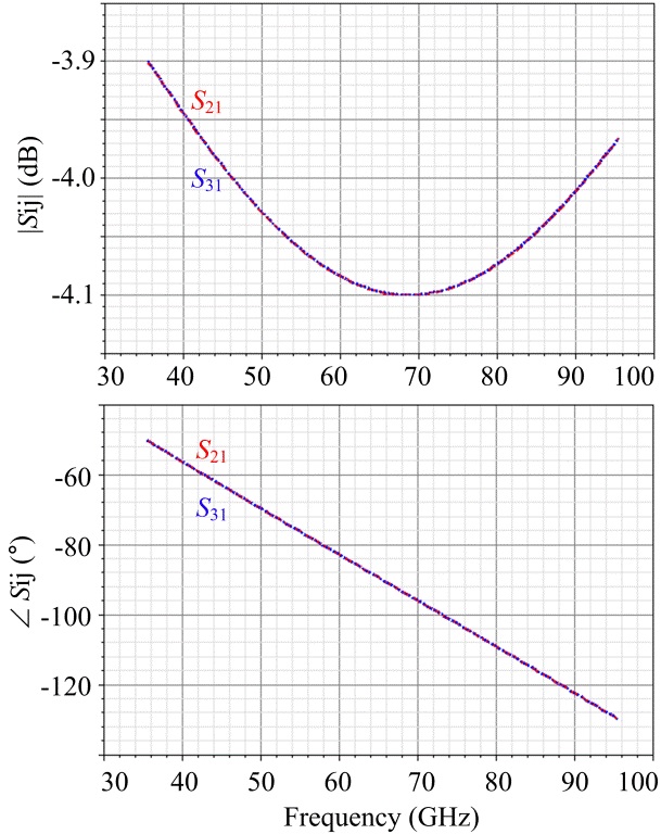
The simulation results, where the power injected to port 1 is divided into port 2 and port 3, are shown in Fig. 6. For the phase shifter, a RF transmission line is utilized since the frequency is high enough that the RF line is short.
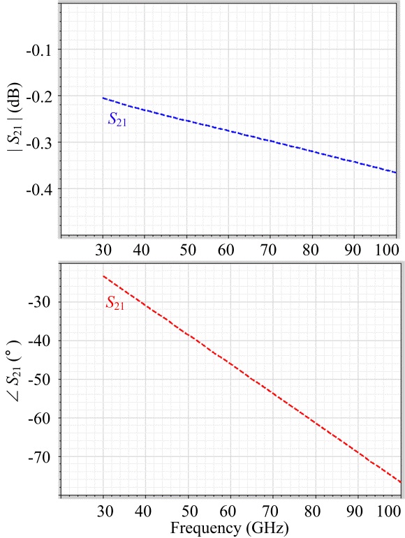
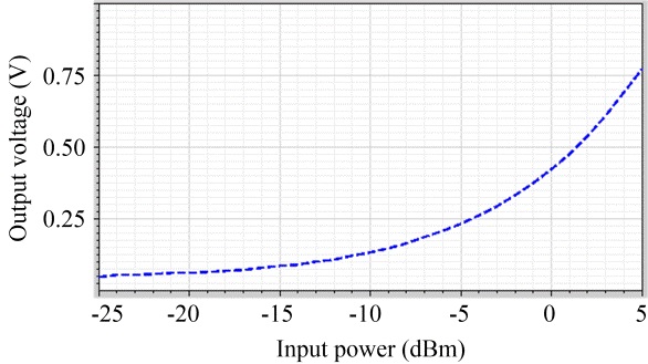
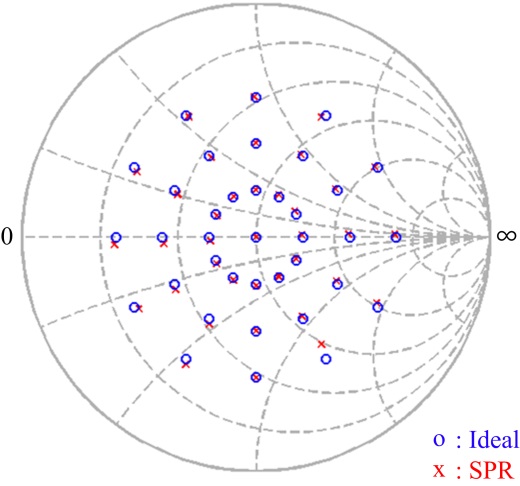
The simulations of the phase shifter are shown in Fig. 7. The phase at 77 GHz is approximately 60°. For the RF power detectors, Lee and Eisenstadt’s power detectors are chosen [27]. Their paper demonstrated detectors working up to 80 GHz in simulation and measuring up to 67 GHz. The simulation results for the single-ended RF power detector demonstrate a power sweep from ?25 to 5 dBm at 77 GHz, as shown in Fig. 8. The simulated reflection coefficient measurement results for 37 well-distributed sample points are shown in Fig. 9. Good agreements are shown in the reflection coefficients between the ideal tuner and the SPR results.
However, a few of the data points do not show good agreement because minor errors in the periodic steady-state (PSS) analysis simulations cause the errors since PSS has a tendency to simplify the simulation process and to amplify minor numerical errors to increase the speed of the simulation.
The embedded RF test circuits, RF power detectors, power control circuits, directional couplers, and a 77-GHz SPR, have been introduced. RF power detectors for embedded RF testing were presented. RF power control circuits were introduced, and directional couplers were presented. The design, theory and calibration techniques for a 77-GHz SPR were detailed. Finally, successful results were demonstrated in simulations. As the importance of testing RF circuits on a chip is increasing, the test circuits for embedded RF testing including the circuits introduced in this paper have wide applicability for modern IC designs.