The explosive advancement of wireless communication devices for multiband and multi-standard applications such as Wi-Fi, WiMAX, Bluetooth, and cellular networks demands low-cost, lightweight, small form factor, and high performance radio frequency (RF) front-end modules. In the multiband or multi-standard devices, the bandpass filter (BPF) is an essential functional block to avoid signal interference between the different bands or standards.
An example of a BPF using surface mountable chip inductors and capacitors is shown in Fig. 1. This design, however, is too bulky to integrate with active components such as amplifiers, mixers, and oscillators in communication devices.
On the other hand, embedded passives are suitable for a system-on-package approach. A variety of embedded BPF design efforts can be found in the literature. A popular design approach is embedding BPF in a low temperature co-fired ceramic (LTCC) such as the interdigital BPF [1] using distributed components or a balanced filter design in a low profile LTCC [2] using lumped circuit elements. Multi-layer organic substrate has been used for embedded passives [3]. Electromagnetic bandgap resonators in a coplanar waveguide [4] or bulk acoustic wave resonators using zinc oxide thin film [5] are used to fabricate a 5 GHz BPF.
In this work, a lumped element LC resonator BPF is designed with a thin ceramic layer in LTCC substrate for coverage of the window of three major WiMAX frequency bands, 5.15?5.35 GHz, 5.47?5.725 GHz, and 5.725?5.85 GHz.
Two different design approaches are considered for the embedded BPF design. One is a distributed BPF design and the other is a lumped circuit element design.
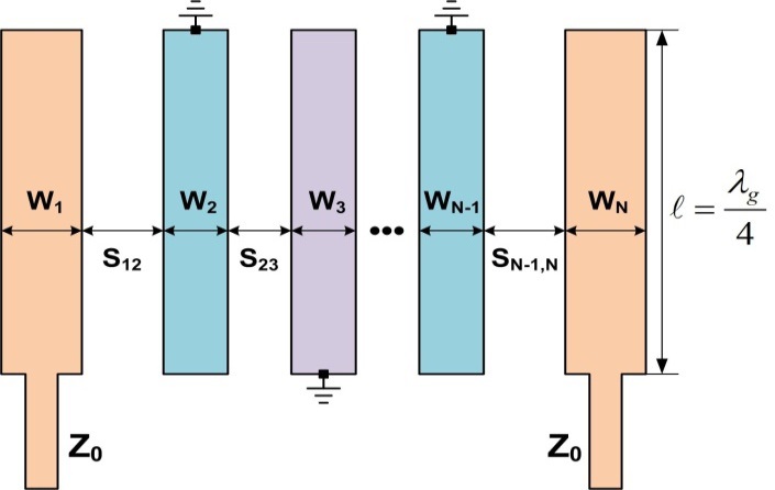
The distributed design approach uses an Nth order interdigital filter described in Fig. 2. The design procedure and relevant equations for the interdigital filter can be found in [6]. Using the design equations in [6], the physical dimensions of the 5th order interdigital filter can be found and summarized in Table 1. The 5th order interdigital filter design is used as a benchmark design in this work. In order to reduce the quarter-wavelength resonator in the interdigital filter design, a high index material, silicon in this work, is used. WN and SN,N+1 in Table 1 are the Nth line width and space between the lines, respectively. The input and output characteristic impedance (Z0 in Fig. 2) is 50 Ω.
[Table 1.] Physical dimensions of the 5th order Interdigital bandpass filter design
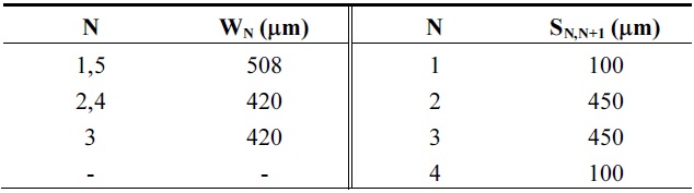
Physical dimensions of the 5th order Interdigital bandpass filter design
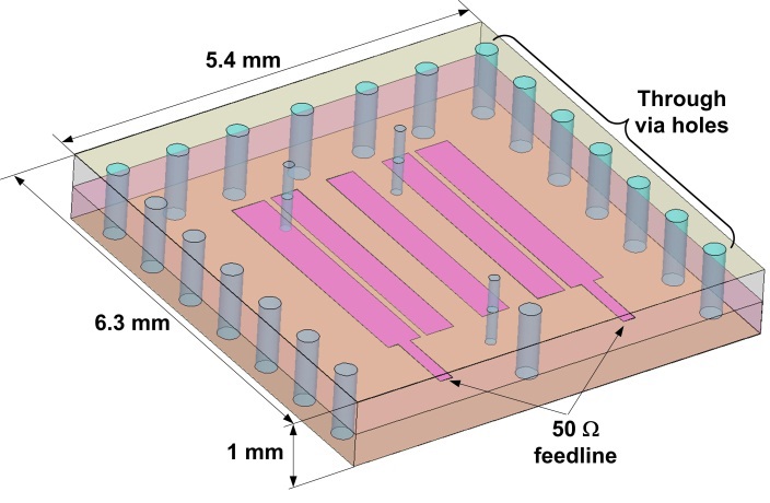
The length ( l in Fig. 2) of the quarter-wavelength resonators at the center frequency of 5.4785 GHz in the passband is 4,002.27 μm. Due to the ground (GND) via holes at the end of the lines, the line length is expected to be shorter than its theoretical value. During the simulation with a three-dimensional (3D) electromagnetic (EM) simulator, High Frequency Structure Simulator (HFSS; ANSYS Inc., Canonsburg, PA, USA), it has been adjusted to be 3,700 μm. The 3D model of the interdigital filter is shown in Fig. 3.
The dimensions of the interdigital filter are much smaller than the bulky BPF design shown in Fig. 1. The volume of the interdigital BPF is 85% smaller than the bulky BPF. To reduce the volume further, a lumped circuit element BPF design with a very thin ceramic layer in LTCC is proposed.
>
B. Lumped Circuit Element BPF Design
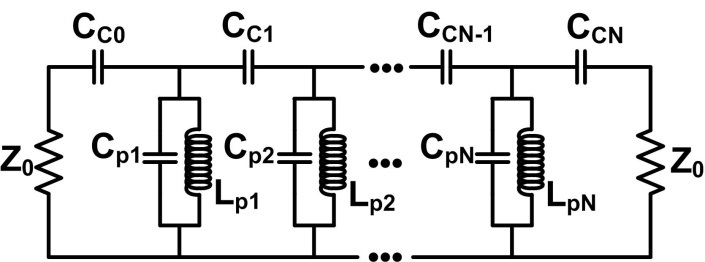
The lumped circuit element approach uses an Nth order capacitively coupled Chebyshev LC resonator filter and is shown in Fig. 4. In order to calculate the component values in the lumped circuit element BPF, a commercial EM design software package, Advanced Design System (ADS; Agilent Technologies, Santa Clara, CA, USA) is utilized. Note that the input and output characteristic impedance (Z0 in Fig. 4) is 50 Ω.
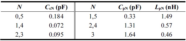
In Table 2, the lumped element values in the BPF design are summarized.
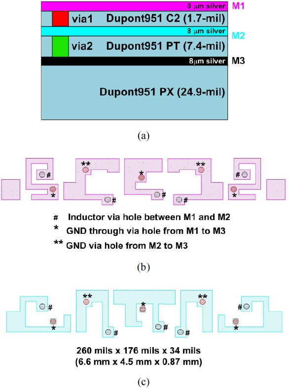
The schematic simulation is performed using the Agilent ADS. For the layout simulation, each capacitor and inductor in Fig. 4 should be modeled in the stack-up substrate. Thus, at the beginning of the design process for a BPF in a multilayer substrate, the configuration of material stack-up must be defined. The LTCC stack-up for the BPF design is determined as shown in Fig. 5a. LTCC uses multi-layer stacking of blue tape with punch holes for through tape connections.
In the layout simulation, the actual shape of the capacitors and inductors in Fig. 4 needs to be determined. In this work, a parallel plate capacitor and spiral inductor are adopted to form the LC resonators. There is a variety of parallel plate capacitor and spiral inductor shapes to consider. Given the stack-up substrate, the 2-layer spiral inductor is an optimal choice because the inductor and capacitor in the LC resonator are in parallel connection, and the LC resonatorbe connected to the universal ground plane. Thus, the via hole connection is an essential part of the whole design.
As mentioned in Section II-A, a very thin ceramic layer (1.7 mils = 43.18 μm) is selected to reduce the area of the parallel plate capacitor, which leads to further miniaturezation of the BPF. In the LTCC design, silver paste was selected instead of gold to reduce material costs. On the bottom of the GND plane (M3 in Fig 5a), a 24.9-mil-thick ceramic layer is used to support the BPF design. Without the supporting layer, it would not be easy to handle the BPF design during the fabrication and measurement process.
The layout design was performed as follows. Indi-vidual capacitor and inductor libraries for the lumped element
[Table 2.] Lumped element values of the 5th order BPF design

Lumped element values of the 5th order BPF design
values given in Table 2 were created in the given stackup substrate by a 2.5D EM layout simulator [8]. Then, the LC resonators were formed and simulated to ensure the designated resonant frequency in the schematic design. Finally, all 5 LC resonators and 6 coupling capacitors were integrated on the same substrate and simulated for the whole BPF design. The layout of the individual components was adjusted during the iteration of the BPF layout simulation to meet the specifications. The typical specifications for a BPF design would be a return loss of 10 dB and insertion loss of 3 dB in its pass band, and attenuation characteristics are given for specific applications.
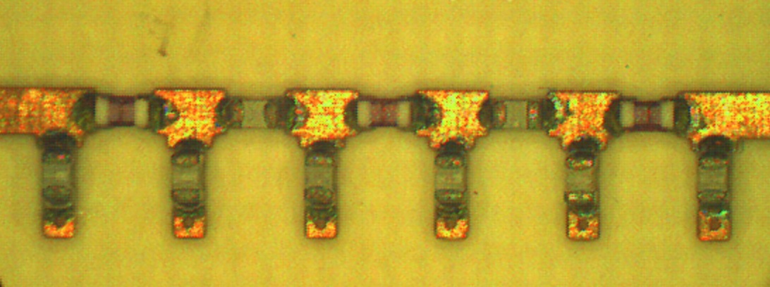
The finalized layout designs are shown in Fig. 5b and c, respectively. There are three kinds of via hole structures in the design. As illustrated in Fig. 5b and c, the first ones (#) are the via holes between M1 and M2 in the spiral inductors. The second ones (*) are the GND through the via holes from M1 to M3. The third ones (**) are the GND via holes from M2 and M3. These via hole structures are common in both silicon and LTCC stack-up substrates.
The physical dimensions of the BPF design in LTCC stack-up substrate is 6.6mm × 4.5mm × 0.87 mm. The BPF design in LTCC stack-up substrate is 24% smaller in volume than that of the interdigital BPF shown in Fig. 3. The volume reduction of the BPF design in LTCC stack-up substrate results mainly from the 1.7-mil-thick ceramic layer. Since the capacitance of the parallel plate capacitors in the LC resonator is inversely proportional to the thickness of the ceramic layer, the thin ceramic layer can increase the capacitance with a given area of parallel plate capacitor. If a 500-μm-thick silicon substrate used in the interdigital BPF design in Fig. 3 is used for the parallel plate capacitors, the area of the capacitor is much larger than the capacitors with the thin ceramic layer due to the substrate thickness.
The results of the EM simulations for the lumped element and distributed design show that the attenuation characteristics of the lumped design are superior to the distributed one.
The 3D and 2.5D EM layout simulators are used to model the interdigital BPF in silicon substrate and lumped circuit element BPF design in LTCC multi-layer substrates, respectively. The material properties for each substrate are as follows: a relative permittivity (
>
B. Performance Comparison Between Lumped Circuit Element BPF Design and Distributed BPF Design
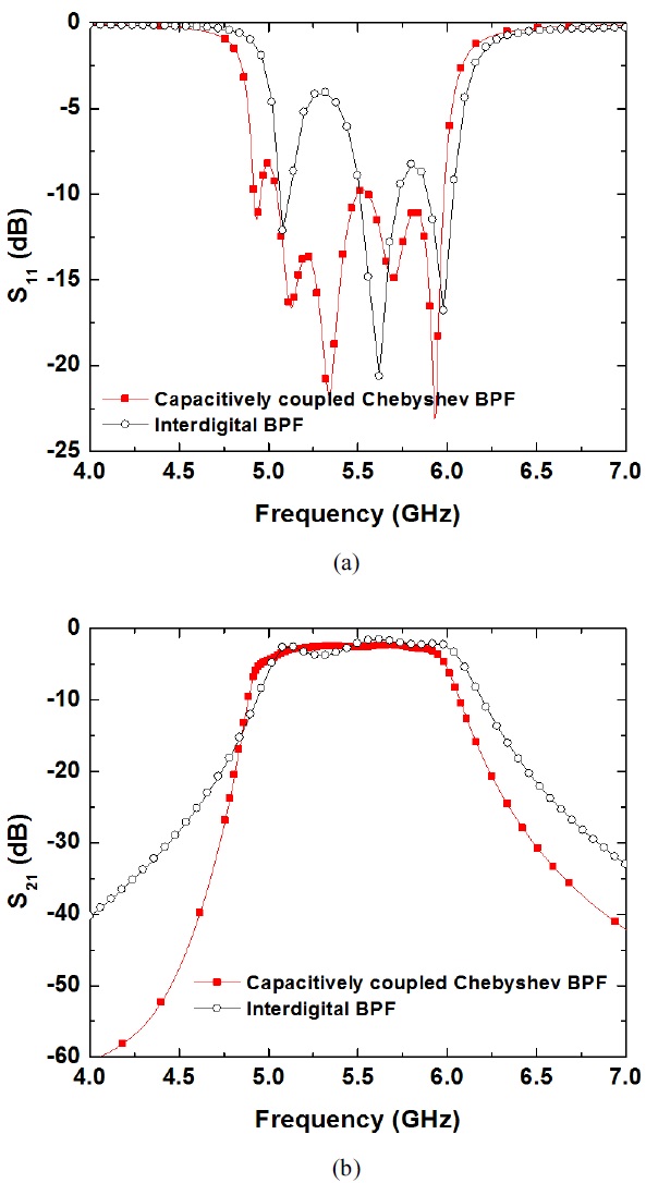
The simulated performance of the 5th order lumped circuit element BPF design was compared to that of the 5th order distributed BPF design for assessment. The return loss (
The results of the EM simulations for the lumped circuit element BPF and distributed BPF design show that the attenuation characteristics of the lumped design are superior to those of the distributed one.
Using the LTCC multi-layer substrate, a compact lumped circuit element BPF has been designed for 5.5 GHz WiMAX applications. It has 5th order capacitively coupled Chebyshev topology, and its physical dimensions are 6.6 × 4.5 × 0.87 mm. The BPF design in a LTCC multi-layer substrate is 24% smaller in volume than the 5th order interdigital BPF in a silicon multi-layer substrate. The EM simulation results prove that the pass band flatness of the lumped circuit element BPF design is better than the interdigital BPF and that its attenuation at 4.75 and 6.25 GHz is 17 and 7 dB superior to the interdigital BPF. The proposed embedded BPF can be a good solution for a compact WiMAX RF front-end module in a system-onpackage.