Wireless sensor networks (WSNs) are enabling ubiquitous technology using data harvested from the environment and obtained from various integrated or external sensors. With such data, we can utilize a series of applications ranging from environmental monitoring systems to surveillance and home automation systems. If the collected data is private and sensitive, privacy issues are of concern.
However, some aspects of WSNs, including wireless communication, resource constraints, and collaborative operation are vulnerable to malicious attacks such as eavesdropping, forgery, and impersonation. Therefore, ensuring network security is the first criterion for running WSN applications successfully and reliably.
Conventional WSN technology uses symmetric cryptography to protect the network from adversaries. However, it poses a number of problems, including those related to key distribution and the number of established keys. WSNs are not suited to these features due to their limited computational power and storage capability because key management impose a heavy overhead on WSNs.
On the other hand, public key cryptography simplifies key management by allowing secure communication by n public key and private key pairs in a network having n nodes. However, this method has been considered to be too burdensome given the resource constraints and limitations of low end sensor nodes [1].
Many studies have been conducted on how to utilize public key cryptography over sensor networks. Among them,
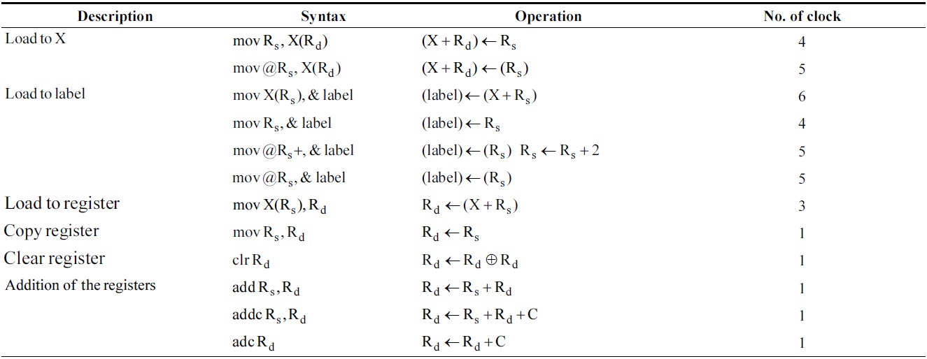
[Table 1.] Instructions of MSP430 used in this paper

Instructions of MSP430 used in this paper
recently [2,3] have shown excellent results using an ATmega128 and MSP430 board. Due to different specifications of sensor nodes, different methods are used for each implementation. [2] uses an operand caching method that maintains the operands using general purpose registers. However, the method does not show high performance on MSP430 because MSP430 has a more efficient hardware multiplier (multiply and accumulation) module. Gouve and Lopez [3] use product scanning methods that maintain the intermediate results to reduce memory access. The results of both works show high performance for executing multiplication. We found that there remains a little room to improve performance by understanding the specifications of the board. In this paper, we review recent multiplication technology and specifications of boards, and then propose more efficient implementation methods.
This paper is organized as follows. In Section II, we give an introduction to the basic architecture of the target processor (MSP430, Texas Instruments, Dallas, TX, USA; ATmega128, Atmel, San Jose, CA, USA) and review previous works on polynomial multiplication. In Section III, we present the proposed multiplication method. In Section IV, we evaluate and analyze the performance of the proposed multiplication method. Finally, in Section V, we conclude with a brief summary of our contributions.
1) Product Scanning
The column-wise multiplication strategy sums up the columns of partial products aj × bj, where i + j = l for column l. Once all the partial products over column l are completed, the content of the lowest register of the accumulator is stored to memory as a part of the result and the other registers are used for accumulation for the next column operation. When column number l increments, multiplication is performed for the next column. This process is repeated until all the partial products have been computed.
2) Operand Caching
This method is a new approach to multi-precision multiplication, in which the number of load and store operations is reduced and the instructions are loaded by reusing operands that have been loaded into the working registers. The method follows the product-scanning approach except that it divides the calculation over several rows. All the needed words of one operand can be cached in the available working registers.
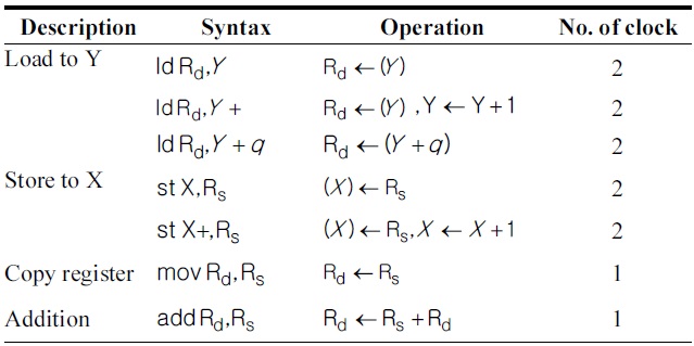
[Table 2.] Instructions of ATmega128 used in this paper

Instructions of ATmega128 used in this paper

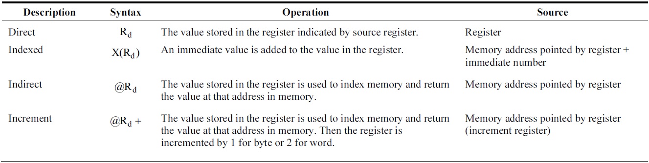
Addressing modes
1) The MSP430 processor
MSP430 is a 16-bit microcontroller clocked at 8.192 MHz including an internal oscillator, timer, hardware multiplier, erasable programmable read-only memory (EPROM), mask ROM, flash memory, RAM, and Joint Test Action Group (JTAG) [4].
The processor consists of 16 registers holding 16 bits each. The registers are numbered from 0 to 15. The first four registers are designated for special purposes and the other registers are general purpose ones.
The MSP430 processor usually provides four addressing modes (direct, indexed, indirect, and increment). The target processor has 27 instruction sets described in Table 1.
The 16×16-bit hardware multiplier is a peripheral that does not affect MSP430 CPU activities. A programmer is able to access a peripheral register to determine operation modes: 1) Multiplication of unsigned 8-bit and 16-bit operands (MPY, address 130h); 2) Multiplication of signed 8-bit and 16-bit operands (MPYS, address 132h); and 3) Multiply-accumulate function (MAC) using unsigned 8-bit and 16-bit operands (address 134h).
2) Architecture of ATmega128
The MICAz mote is equipped with an ATmega128 8-bit processor clocked at 7.3728 MHz. It has a 128 kB electrically EPROM (EEPROM) chip and 4 kB RAM chip [5]. The ATmega128 processor has reduced instruction set computer (RISC) architecture with 32 registers. Among them, 6 registers (r26-r31) hold the special pointers for indirect addressing. The ATmega128 has a 16-bit addressing scheme that requires two registers for the address alone. The remaining 26 registers are available for arithmetic operations. One arithmetic instruction costs one clock cycle, and memory instructions or memory addressing costs two processing cycles. Table 2 illustrates the instructions, including arithmetic, logical and register control, and data instructions.
3) Addressing Mode
Both architectures provide four different addressing modes. First is the direct mode for accessing the destination address directly. Second is the indexed mode, which is similar to array access in the C language. The destination can be accessed with the addition of a source and offset. The third mode is the indirect mode, which accesses the destination by using registers, so it executes more efficiently than memory access. The last mode is the increment mode, which has the strength of computing the address automatically after accessing the address when destinations are sequentially placed in memory.
III. IMPLEMENTATION TECHNIQUES
In this section, we propose implementation techniques. The main idea is accessing memory only a small number of times and removing reducible operations. We used previous multiplication methods, operand caching, and product scanning for the ATmega128 and MSP430, respectively.
>
A. Operand Caching Using General Purpose Registers
Memory access operations consume more clock cycles than register-based operations. Therefore, replacing memory operations with register operations efficiently improves performance. In the implementation, we maintained the values in the registers and reduced memory access. In the MSP430, 6 registers are used for operand caching and in the ATmega128, 20 registers are used for operand caching. Through the partial product, some portion of present and future operands overlaps. In this case, we just maintained the value in the registers and reduced additional operations.
To enhance the performance of polynomial multiplication over that of the MSP430, we have used the increment addressing mode as much as possible because the increment address mode can save 1 clock cycle in the address calculation time. That is, it can save the time for calculating the next instruction or data to be fetched. When saving the result, we used the index mode, which easily computes the destination from the source address with an offset.
For the ATmega128, we used the index mode for load and store operations. The ATmega128 makes no distinction between index and increment modes, so the addressing mode is not of particular concern.
To store the intermediate results, we maintained registers for accumulation. The registers should be first initialized, but we stored the result instead of using the clear and addition operation. The first and last partial products do not generate a carry, so we do not need to initialize the registers in those cases. Through these procedures, we were able to optimize the number of clear operations.
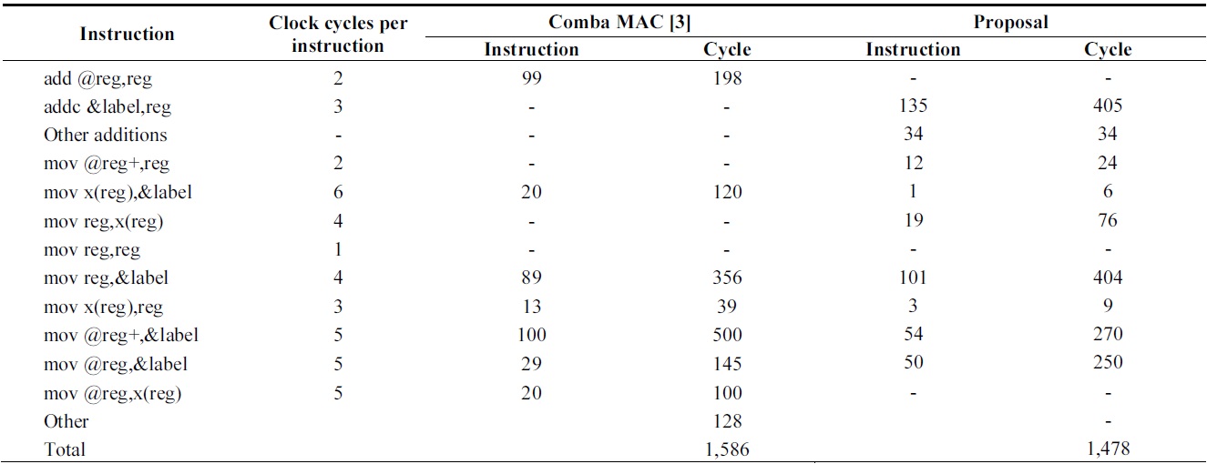
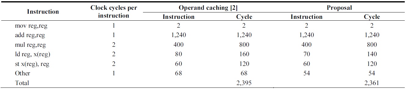
[Table 4.] Comparison of instruction counts of 160-bit multiplication over MSP430

Comparison of instruction counts of 160-bit multiplication over MSP430
[Table 5.] Comparison of instruction counts of 160-bit multiplication over ATmega128
Comparison of instruction counts of 160-bit multiplication over ATmega128
Tables 4 and 5 show the results of multiplication using MSP430 and ATmega128, respectively. The MSP430 shows great improvements by using register caching and efficient address modes. Therefore, the number of times that memory is accessed is reduced and reducible addressing operations are removed.
In the case of the ATmega128, the load and store instructions are reduced by maintaining intermediate results. Secondly, the clear operations for register initialization can be minimized considering the cases in which cache is not generated. The detailed instructions are presented in Table 5.
In the paper, we show the efficient implementation techniques by using the unique specifications of the target board. By using an efficient addressing mode and general purpose registers, the performance is improved in both architectures. The information described in the paper could be used for many other implementations in security and graphics processing modules.