Recently, liquid crystal displays (LCDs) have been widely used in various applications because of their high performance specifications, such as lightness, high resolution, and low power consumption. There are several popular modes for LCDs, such as the twisted nematic mode, the vertical alignment mode, the in-plane switching mode, and the fringe-field switching (FFS) mode [1-5]. With the recent increase in demand for display devices exhibiting a high pixel density to provide high quality images and wide viewing angles, more attention has been given to the FFS mode [6-8].
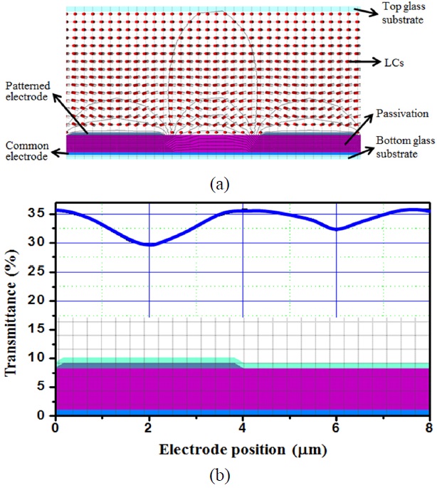
The FFS mode exhibits a wide viewing angle because the liquid crystals (LCs) are homogeneously aligned initially and subsequently rotated within a plane parallel to the substrates by applying the fringe-electric field. In the FFS mode, since a passivation layer is located between the common electrode and the patterned electrodes, an additional storage capacitor is not required and in turn a high aperture ratio is maintained.
Although the FFS mode offers these advantages, this mode shows a relatively slow response in comparison with the other LC modes, such as vertical alignment and twisted nematic modes, because the switching time of the FFS mode primarily depends on the elastic constant
In this paper, we propose a protrusion structure to realize a fast response time in the FFS mode. We form the protrusion on top of the passivation layer between patterned electrodes, where light is not modulated by the phase retardation effect, resulting in little decrease in the transmittance. Given that the protrusion structure can reduce the effective cell gap, we can expect that the fast response time can be achieved while maintaining the transmittance at nearly the same level as that of the conventional FFS mode without the protrusion structure.
II. CHARACTERISTICS OF THE FFS MODE
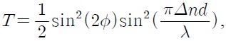
In the FFS mode, the transmission of light is expressed by the following equation:
where
is the birefringence of the liquid crystal medium, and
III. PROPOSED STRUCTURE FOR FAST RESPONSE TIME
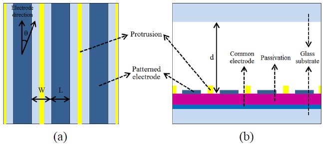
The proposed structure to reduce the response time is
shown in Fig. 2. On top of the bottom substrate, rectangular protrusions were formed between the patterned electrodes. For numerical calculation of the electro-optic characteristics of the proposed structure, we employ a commercial software package “TechWiz LCD 3D” (Sanayi System). The parameters for numerical calculation are as follows. The thickness of each ITO electrode layer is 0.06 μm. The thickness of the oxide (
IV. CALCULATED RESULTS AND DISCUSSION
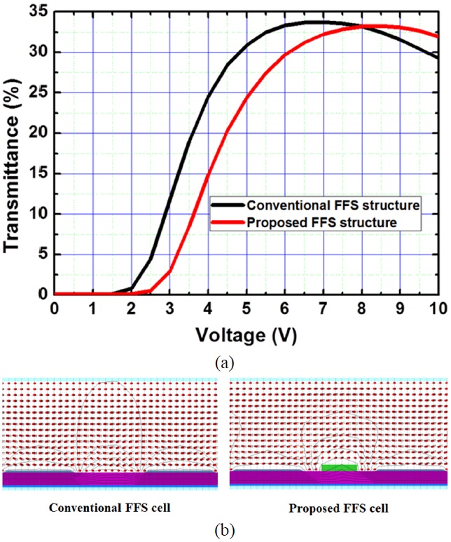
The voltage-transmittance curves of the conventional and the proposed structures are shown in Fig. 3(a). The maximum transmittances of the conventional and the proposed structures are 33.8% at 6.8 V and 33.2% at 8.2 V. The transmittance of the proposed structure was almost the same as that of the conventional structure. To better understand why the proposed structure can have almost the same transmittance as the conventional structure, we calculated the distribution of the LC directors and equipotential lines at maximum transmittance. Fig. 3(b) shows the cross-sectional views of the LC director profiles in the conventional and the proposed structures at maximum transmittance. Because the protrusion is formed in the region where light is not modulated by the applied field, there is only a slight decrease in the transmittance attributed to the formed protrusion.
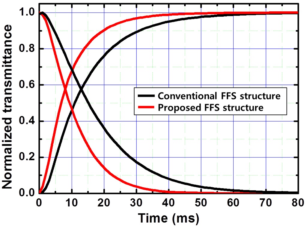
We calculated the response times of the conventional and the proposed structures. The rise time is defined as the time required for the optical transmittance to change from 10% to 90% of the maximum transmittance, and the decay time is defined as the time for the optical transmittance to change from 90% to 10% of the maximum transmittance. Fig. 4 shows the calculated response times of each structure. The response times of the proposed structure are much faster than those of the conventional structure. In general, the turn-off time of the FFS mode is inversely proportional to the twist elastic constant
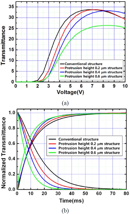
To confirm the low cell gap effect attributed to the protrusion structure, various heights of the protrusion were assumed for a fixed width of 1 μm. It was observed that as the height of the protrusion increased, the transmittance decreased. For heights of 0.2, 0.4, and 0.6 μm, the transmittance was decreased by 0.1%, 0.2%, and 15.7%, respectively, as shown in Fig. 5(a). Because a higher protrusion can make it more difficult for LCs to be rotated, light is
less modulated by the phase retardation effect. Although the transmittance decreases with an increase in the protrusion height, the total response time is 19%, 33.5%, and 41.5% faster than that of the conventional structure, as shown in Fig. 5(b). As the cell gap at above the protrusion decreases
[TABLE 1.] Dependence of the transmittance and response time on the protrusion shape
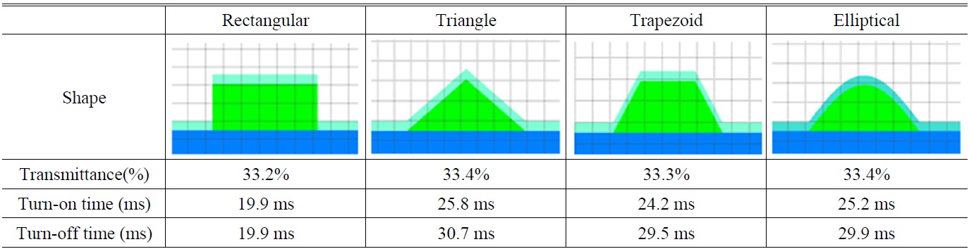
Dependence of the transmittance and response time on the protrusion shape
with the formation of a higher protrusion, the response time can be reduced by the low cell gap effect. In case the height of protrusion is lower than 0.4 μm, the reduction of the transmittance is smaller than 0.2%. However, when the height of protrusion is greater than 0.6 μm, the transmittance is drastically decreased (15.7% compared with the conventional structure). So we decided to use 0.4 μm condition as the optimized condition.
Next, we calculated the light leakage in the dark state. There was only a slight leakage of light caused by protrusion in the dark state, therefore both the cells had almost the same dark levels. These results were obtained because the rubbing process was made along the protrusion structure. We studied the dependence of the response time of the proposed structure on the shape of the protrusion. For a fixed width of 1 μm, we considered several protrusion shapes, such as a triangle, a trapezoid, an ellipse, and a rectangle, as shown in Table 1. Because of the low cell gap effect, a fast response time was achieved in each of these structures, also shown in Table 1. Among them, the rectangular structure showed the highest enhancement of the total response time (33%). The most proper structure for the proposed method is rectangular because the surface of the rectangular structure is uniformly flat. Therefore, we can obtain low cell gap effect perfectly by forming a rectangular structure. However, other structures of protrusion do not have a flat surface. Therefore, enhancement in the response time of other protrusion structures is less effective. However, the other structures also exhibited a faster response time than those of the conventional structure, while minimizing the decrease in the transmittance.
Actually, insertion of protrusion between patterned electrodes may not be an easy job in the manufacturing process. However, protrusion technology has been already used in the MVA or IPS mode [13,14]. Therefore, we believe that the proposed method can be a useful method to reduce the response time in spite of the difficulty in fabrication.
In conclusion, we proposed a cell structure for an FFS cell to achieve a fast response time, with only a slight decrease in transmittance. We formed a protrusion structure on the bottom substrate in order to reduce the response time by the low cell gap effect. By optimizing the shape of the protrusion structure, the total response time can be decreased by 33% with little loss of the transmittance. We expect that the proposed cell structure will contribute to the realization of fast-response LCDs.