As the semiconductor industry grows rapidly, the size of semiconductor devices is getting smaller and the degree of integration of semiconductor devices must be higher. Gradually, the pattern of the semiconductor device’s integrated circuit is getting finer and the precise fabrication of the photo-masks is essential.[1~3]. Recently, short wavelength light sources such as ArF excimer laser at 193 nm wavelength are used for lithography to make a high resolution pattern on a microelectronic semiconductor device [4]. By the high photon energy of an ultraviolet light source such as an ArF excimer laser, various photo-mask pollutions like hazes appear on a photo-mask due to photochemical reactions among SiO2, H2O2, NH4OH, etc. Small defects formed by the solidification of the reacted gases could cause critical problems on the photo-mask’s surface: the pollutants grown could randomly block or connect the patterned lines, resulting in a large number of defects in the forth-coming lithography process. [5]. Therefore, in-situ optical inspection of photo-mask’s defects with a submicrometer resolution is of great importance to prevent the possible growth of defects as the subsequent processes go on. The inspection system should be designed to satisfy all the requirements of the semiconductor industry: high measurement speed, wide inspection area, small system footprint, and low price.
In this paper, we designed and developed an on-axis optical inspection system by means of the interference between the scattered light from the sub-micrometer defects with the reflected light from other clean parts of the reference surface: our method offers high-speed inspection, high resolution, vibration-insensitivity as well as a high visibility of the interferogram.
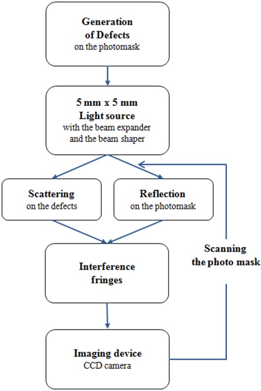
II. DESIGN CONCEPT OF NEW OPTICAL DETECTION SYSTEM
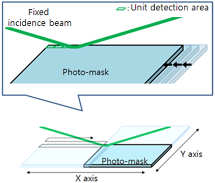
The basic process of our in-line inspection is as shown in Fig. 1. The overall system is composed of the optical detection system, the mechanical scanning system and the
image processing software. To scan the whole area of the photo-mask with the square size of 6 inch × 6 inch, the photo-mask moves right and left and/or back and forth by using a motor-controlled home-made mechanical linear 2 dimensional stage with an accuracy of 0.5
The incident beam propagates to the defects on the photomask and is separated into three parts on the photo-mask; two of them are reflected light from the front surface and the rear surface of the photo-mask passing directly toward the image device and the other is light transmitted through the photo-mask. By using appropriate methods such as separating two reflected beams laterally by the use of a thick photo-mask and blocking reflected light from the rear surface of the photo-mask, the transmitted light which passes through a photo-mask and propagates in opposite direction is removed and has no influence on the image quality. The weak scattering light of spherical wavefront from defects and the strong reflected light of plane wavefront from the front surface of a UDA on the photo-mask’s glass plate without any defects propagate to the imaging device of a charge coupled device (CCD) camera. If the intensity ratio of two lights can be well controlled by appropriate optical methods, then interferograms can be obtained at the CCD camera as a result of the interference [6,7]. Hence, the existence and position of the defects on a UDA will be found out easily by the visual analysis of detected interference fringes.
2.1. Optical Configuration Using Interference Method
A Gaussian beam of 1.00 mm diameter is expanded and shaped to a flat-top beam of 5 mm × 5 mm on a UDA by using a beam expander, a beam shaper and a square mask. Since the size of the defects is much smaller than the size of the photo-mask area without defects inside the cross section of the incident beam, the intensity of the scattered light from defects is very weak and the intensity of the reflected light from a photo-mask’s surface without any defects is relatively much stronger than that of scattered light. In the general case, due to the great difference between the intensities of two different kinds of light generated from a photo-mask with defects, the visibility of interference fringes is too poor to be detected directly by a visual method. For good contrast, two light intensities of the scattered light and the reflected light have to be nearly the same [7].
In this paper, as the wavelength of the laser light source is nearly the same with the defect whose size ranges from several hundreds of nanometers to several micrometers, Rayleigh scattering can be applied in our case as described in Eq. (1) [8,9] :
where
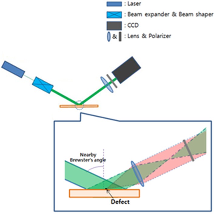
To dramatically reduce the intensity of the strong reflected light for good contrast of the interference fringes the incident laser beam is incident at the incidence angle nearby the Brewster’s angle to make a very weak p-polarization component of reflected light and to get mainly rid of an s-polarization component of a strong reflected light and a weak scattered light with a p-polarization component [11]. By this method, the weak intensities of a reflected light and a scattered light with p-polarization in front of the CCD camera can be approximately adjusted the same. To match these two intensities more closely, a convex lens is put at an available position between the photo-mask and the CCD camera along the optical axis. One role of the lens is the additional decreasing of the reflected beam intensity by the convergence and divergence
of the beam as it passes through the back focal point of the lens and diverges to cover a CCD camera. The other important role of the lens is to minimize the loss of the scattered light by focusing the light to the CCD.
As a result, the scattered light and the reflected light with p-polarization on a UDA, which are controlled for two beam intensities to be nearly the same, make interference fringes with a good visibility on the CCD camera. The schematic diagram of equalizing light intensities between the reflected and scattered beams is shown in Fig. 2 in detail. This system is not affected by external mechanical vibrations because of the propagation from two sources of light for interference along the same optical axis from the same originating wave sources of a photo-mask.
2.2. Mechanical Scanning System and Image Processing Software
To inspect whole area of the photo-mask, the photo-mask needs to be scanned along two orthogonal axes because the size of photo-mask is much larger than the UDA on the photo-mask. The size of a square photo-mask is 6 inch × 6 inch, the effective size of total detecting area is 150 mm × 150 mm, located at the center. As 30 UDAs along a row, the X-axis which is a horizontal axis, and 30 rows along the column, the Y-axis which is a vertical axis, have to be measured on a photo-mask, we have to measure 900 UDAs, exactly. The moving direction of the scanning detection system is designed to move from left to right through columns along the first row, then shifting by one row, then from right to left through columns along the next row as shown in Fig. 3. Since the time of operation at a detection area including the time to transfer from a UDA to the next neighboring UDA is designed to about 2
seconds or less, the total operating time for one 6 inch × 6 inch photo-mask detection may be determined to be less than 30 minutes.
2.3. Key Ideas of Image Processing Software
The key ideas of image processing software are to make the higher contrast of the image as a result of reducing the background noise of a captured image, to handle easily the direction of a unit detection image (UDI) on the CCD camera, to fit the size of a UDI to the size and position of a UDA, and to stitch 900 UDIs and complete the detecting image of an entire photo-mask. To remove background noises generated by scratches, dusts, and bubbles on many optical elements on the optical system on a detecting image, the method to subtract a reference image (RI), which is obtained by a reference photo-mask without defects, from a UDI with some interference fringes is used.
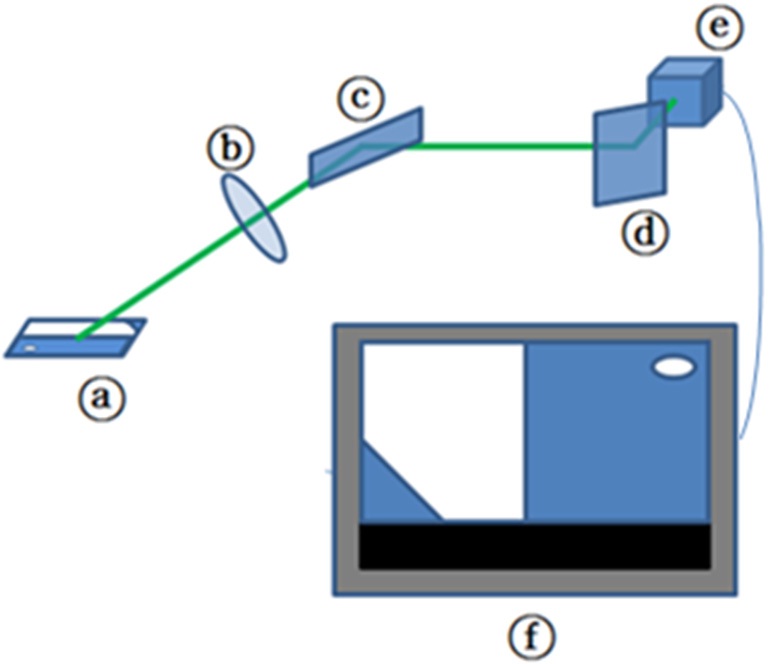
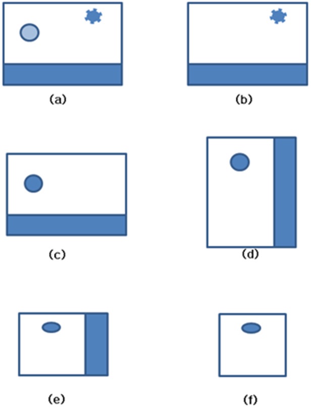
As shown in Fig. 4 noting the position of various patterns on a UDA, the position of patterns (ⓐ) on a UDA is rotated 90° clockwise and reversed with respect to a vertical axis of the photo-mask to a CCD camera as shown in the interference image on the monitor (ⓕ) by a lens (ⓑ) and 2 mirrors (ⓒ and ⓓ) to set up for controlling of the ratio of intensity of two beams and folding two beams toward a CCD camera (ⓔ) fixed on the bread board. As a result, the position of various patterns at the CCD camera can be observed in the monitor as shown in ⓕ. Simultaneously, a square shaped UDA changes to a rectangular shaped UDI including any useless edge images due to the oblique effect of the photo-mask with respect to the CCD camera. So both the position and the size of the deformed UDI on a CCD camera have to be transformed to the image shape and the position of patterns on an original UDA.
Figure 5 shows the flow chart of image processing to solve various problems of an image rotation and transformation generated by several causes shown in Fig. 4. The first step is to subtract (b) an RI from (a) a UDI image on
the monitor to remove the background noises and to get the high image contrast as shown in (c). The second step is to rotate the image 90° counterclockwise and reverse with respect to the horizontal axis of the image to correct the position of a UDI to that of a UDA. The third step is transforming (d) a pressed image along the X axis into (e) an original image to correct the size of an image deformed by the incidence angle. The fourth step is to trim the useless edge parts of a UDI from the image of (e) as 5 mm × 5 mm. Finally, a UDI of (a) becomes (f), a complete
image with a clear image quality, correct size and correct direction.
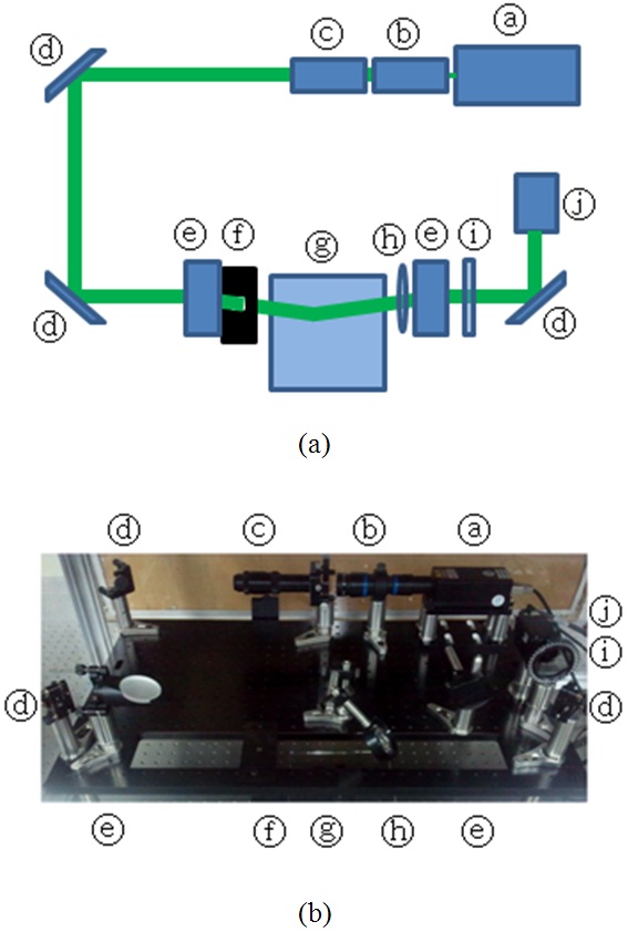
The experimental system is implemented based on the design concept as explained in Section II. Fig. 6 shows (a) the schematic diagram and (b) the photo of the optical detection system. In order to get the higher intensity of scattered beam for the detection of bright and clean interference images, we chose the green laser (
Because our inspection system will be installed as a part of the lithography equipment, the second harmonic wave generated from the diode pumped solid state (DPSS) Nd:YAG green laser (PHOTOP, DPGL-2200) as shown in ⓐ of Fig. 6, with the power of 200 mW is chosen for compact size and suitable power.
To make the incident beam with a uniform flat-top intensity on a photo-mask, the beam expander (JENOPTIK, Beam Expander 2x-10x 017052-201-26) (ⓑ) and the collimating beam shaper (MOLTECH, piShaper_6_6_532/ 1064) (ⓒ) are set up as shown in Fig. 6. The beam expander expands the diameter of incident beam to φ 6 mm enough to cover a UDA on the photo-mask. Then, the beam shaper changes the expanded Gaussian beam into the flat-top beam with the fluctuation of beam intensity of less than 5%. Three corner mirrors (ⓓ) are placed on the corners of the board and two folding mirrors (ⓔ) are used to fold the incident beam to the photo-mask nearby Brewster’s angle and to propagate the reflected and scattered lights to a CCD camera. The Brewster’s angle is θB = 55.59° according to the refractive index (nquartz = 1.46) of the photo-mask made of quartz.
The multi-reflection is naturally generated by reflection at the front surface and the rear surface of a photo-mask near the Brewster’s angle. If a photo-mask is thinner than 4 mm, then the reflected light on the rear surface will superpose partially to the reflected light on the front surface. As a result, linear Fizeau fringes are generated by an interference effect. To remove these fringes completely, the reflected lights from the front surface and the rear surface of the photo-mask have to be separated by using a thick enough photo-mask. The thin square mask of 6 mm × 6 mm bigger than 5 mm × 5 mm is put carefully onto the photo-mask for making a square UDA of 5 mm × 5 mm on a photo-mask from the circular beam. The reasons for using a square mask of 6 mm × 6 mm is to get rid of the edge diffraction effect of the mask to get the clean UDI of 5 mm × 5 mm. After being reflected on a photomask, the reflected light from rear surface has to block by using a black blocking plate. The conventional 6025 photomask of a blank quartz plate (ⓖ) which has the width of 6 inch, the length of 6 inch, and the thickness of 0.25 inch (6.35 mm), is enough to separate the two reflected lights. However, after being reflected at the photo-mask, the flat-top square beam becomes a rectangular beam in consequence of the oblique reflection near Brewster’s angle. In this circumstance, while the very strong reflected light is composed of almost all an s-polarization component, the very weak scattered beam from defects has almost equally s-polarization and p-polarization components.
And a convex lens (Melles Griot, 01 LDX 205) (ⓘ) with the focal length of 150 mm is used to make the intensities of the reflected light and scattered light the same for the good visibility of interference fringes. The center of the photo-mask is placed at the focal length of a lens along the optical axis. Due to the inclination of the photo-mask at θB = 55.59°, the optical path difference (OPD) from lens to both sides of a UDA along the optics axis with respect to that from the center of an UDA to the lens is ± 2.06 mm. Since the maximum variation error of the OPD is a mere 1.38% with respect to the focal length of 150 mm, we can assume that the variation of the OPD is negligible. Therefore, all lights outgoing from defects have almost equal spherical wavefronts. The intensity of very weak scattered light with all polarization components from defects is almost not changeable because the scattered light is collimated to the CCD camera by the convex lens, which places it at the same distance as the focal length of the lens. The reflected beam on a photo-mask is focused and diverged in turns by the convex lens and so the size of it is bigger than that of the image device. Total intensity of reflected light with very strong s-polarized component and very weak p- polarized component can be controlled by the position of the CCD camera and the change of lens power. Since we can get rid of the strong s-polarization component of scattered light and also the s-polarization of a reflected light by using a linear polarizer (ⓙ), we can control precisely the ratio of intensities of reflected and scattered light until the ratio is nearly 1:1 for the good visibility of interference fringes.
In this system, a CCD camera (CIS, VCC-G32S11CL) with 1392 × 1040 effective pixels in the size of 2/3 inch (that is, 8.98 mm × 6.7 mm) is utilized as an imaging device. In front of the CCD camera, a linear polarizer is located to filter out the strong s-polarization component of the reflected beam and the weak s-polarization component of the scattered beams. As a result, we can observe clearly and distinctly interference fringes in a UDI because the polarization state and intensities of two lights without s-polarization components is well matched for a good visibility of fringes.
The schematic diagram and photograph of the experimental setup of the optical system is shown in Fig. 6 in detail.
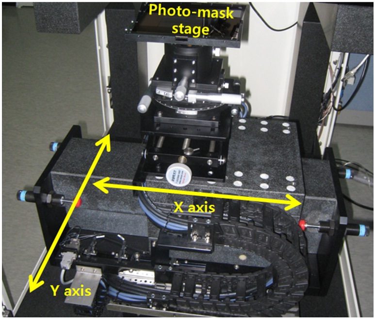
The mechanical scanning system with custom-built photomask stage to move the photo-mask is installed under the fixed optic system on a bread board as shown in Fig. 7. The driving motor of the x axis for the movement along the row of the photo-mask is chosen as the linear servomotor (ATL26G 160 / G28-101) with the air-bearing. The other motor of the y axis for the movement along the column is chosen the linear stepping motor (ATL25B 460 / MB04NH). Each motor is differently chosen by considering the weight of above, the operation length, etc. Linear accuracy, that mean the repeatability, of the mechanical scanning system along the x axis and the y axis is ± 0.5
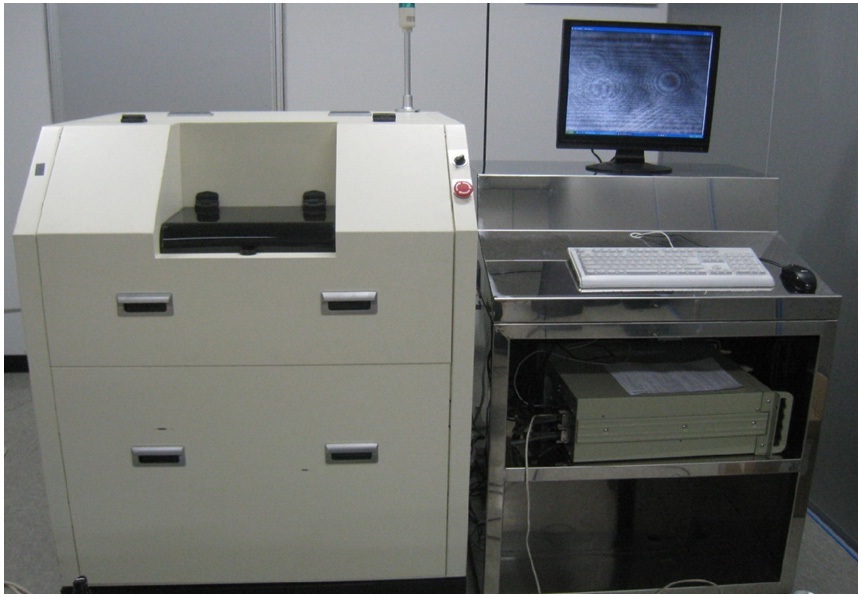
The photograph of the operating experimental setup of the new scanning detection system is shown in Fig. 8.
IV. EXPERIMENTAL RESULTS AND DISCUSSION
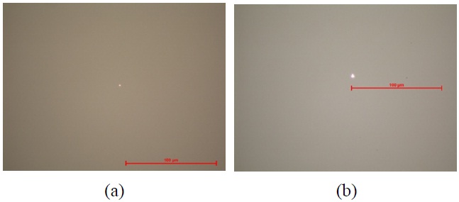
To evaluate major performances of the detection system for the detection of defects on a photo-mask, the artificial test defects instead of actual defects including hazes are made on 6025 photo-mask blank quartz plate with the size of 6 inch × 6inch and the thickness of 0.25 inch. The total size of the scanning detection area to sculpture artificial test defects is 150 mm × 150 mm. One of the test defects is made by spreading optical polishing powder made of cerium oxide, CeO2, on the photo-mask instead of various metal or dielectric test defects fabricated on the blank plate of photo-mask for the simple and fast preliminary test. For the case of CeO2, although the diameters of the single cerium oxide particles are less than 3
minimum defect size, respectively, where
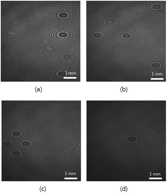
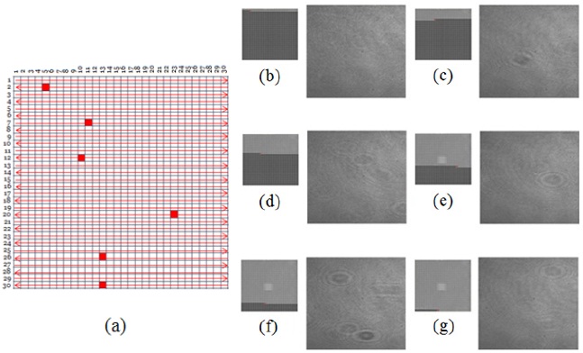
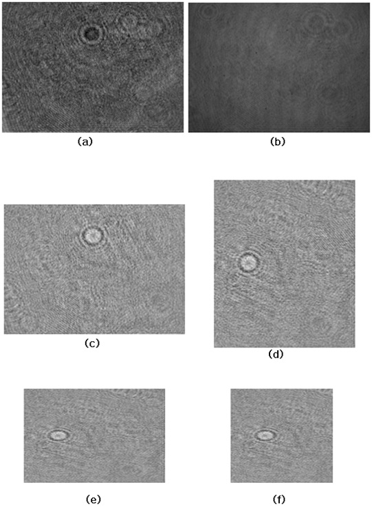
Figure 10 shows detected images of several UDAs selected through the scanning process over whole photomask inspection area of a photo-mask, consisted of 900 UDAs for the case of CeO2 powder. In order to check the scanning function of the system, we chose six scanning positions, represented by red boxes in Fig. 10(a), on 5th row on 2nd column, which is represented by (5, 2), 11th row on 7th column, (11, 7), 10th row on 12th column, (10, 12), 23nd row on 20th column, (23, 20), 13th row on 26th column, (13, 26), and 13th row on the last column, (13, 30). As shown in the small left photo of Fig. 10(b) ~ (g), the red mark of each photo represents different UDAs of a photo-mask and the right large photos of Fig. 10(b) ~ (g) are images of each UDA on each of these positions. We can see a lot of interference fringes placed at random positions in these UDIs because we arbitrarily spread CeO2 powder on a photo-mask without patterns. We confirm that there is no problem to control artificially the position of a UDA as shown in Fig. 10.
Figure 11 is all images obtained by each step of image processing as following in the flow chart of image processing software explained in Section 2.2 for CeO2 powder. By the suitable image processing software, the size of image has to resize to 5 mm × 5 mm and correct toward the same direction of the photo-mask on the monitor for the useful assembling of an entire detecting area. As a result, in case of a UDI, we obtain clear images (Fig. 11(c)) by reducing background noises by the method to subtract the reference image (Fig. 11(b)) from a captured original UDI (Fig. 11(a)). And we rotate its orientation (Fig. 11 (d)) to 90° counterclockwise and decompress the image of Fig. 11(e) to the scene of a detecting image (Fig. 11(e)). Finally, as the size of corrected image (Fig. 11(e)) is slightly different from that of CCD device, we have to reform the size of a UDI as 5 mm × 5 mm by the removal of useless edges and coincidence with each boundary of all UDIs as shown in Fig. 11(f).
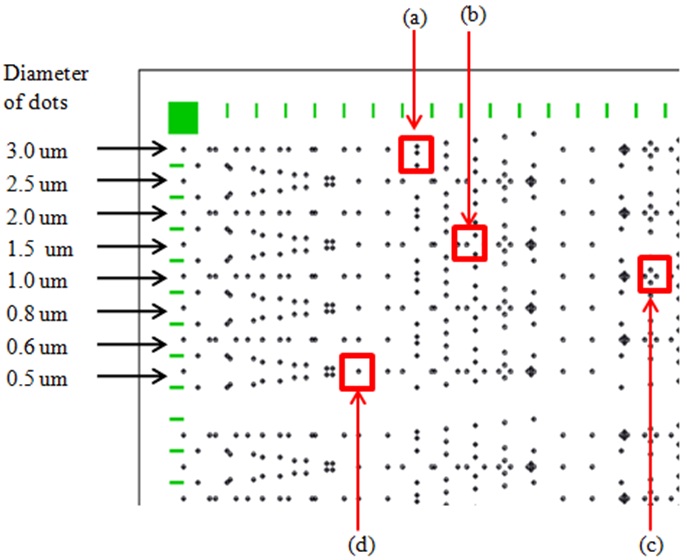
Figure 12 shows the dot pattern on a photo-mask for Al test defects with various diameters of (a) 3.0
The use of the ArF excimer laser in lithography causes pollutants including haze on a photo-mask by various photochemical reactions. In order to detect and eliminate the polluted sections of photo-mask, we need a new optical scanning detection system to detect the defects in order to save the detecting time and adjust the size of the detection system to the mass producing system. In this paper, a defect detection system of a good performance with the total working time within 30 minutes and total scanning square size of 6 inch × 6 inch using interference effect on an axis of scattered lights on defects and a reflected light on a photo-mask is proposed and fabricated to inspect the hundreds of nanometer and micrometer defects. This system is using the interference effect generated by the superposition of two lights propagating along an equal axis and causing strong external mechanical vibrations to a photo-mask resist.
To evaluate the defect scanning detection system, test defects were made of cerium oxide optical polishing powder and Al dots on a photo-mask of 6 inch × 6 inch. All of the test defects from the size of 0.5