In an optical Rx design, the TIA plays the role of a front-end amplifier for amplifying the weak current signals generated from the photodiode (PD) and converting to voltage signal which would be fed to a subsequent block (limiting amplifier or clock and data recovery circuit). The conventional Rx consists of a TIA preamplifier block, limiting amplifier, and the output buffer. There are several works that have reported on 10 Gbps front-end optical receiver designs [1-7]. Bandwidth enhancement techniques using inductive peaking has been proposed [1-5] for designing high data rate operation of an optical Rx. However, an excessive size of the inductor makes the chip big and expensive. An inductorless TIA has been designed in [6], where several shunt feedback TIAs connected in parallel were suggested for bandwidth improvement and chip size reduction. This design method has high power consumption due to the several TIAs deployed. The bandwidth enhancement technique for transimpedance amplifiers using capacitive peaking which has been realized using a single capacitor is a good candidate for small-area TIA design [7]. However, the negative capacitance is directly loading to the input of the TIA, therefore introducing high peaking at the transient response of TIA. We therefore propose an inductorless TIA that functions as an optical Rx, which does not require a limiting amplifier stage, thereby reducing total chip size. In our proposed design, the RGC input stage has been utilized with post amplifying active feedback amplifiers to lower the input capacitance of PD and for bandwidth improvement. A high gain-bandwidth product per DC power figure of merit of 408 GHzΩ/mW is achieved with the combination of passive (resistive) and active (NMOS transistor) feedback components. Thus, the absence of inductors in the proposed TIA-Rx results in a power efficient chip with small size. In this work, a 10 Gbps TIA-Rx chip that operates up to 10 Gbps have been designed and fabricated in a 0.13 μm CMOS technology.
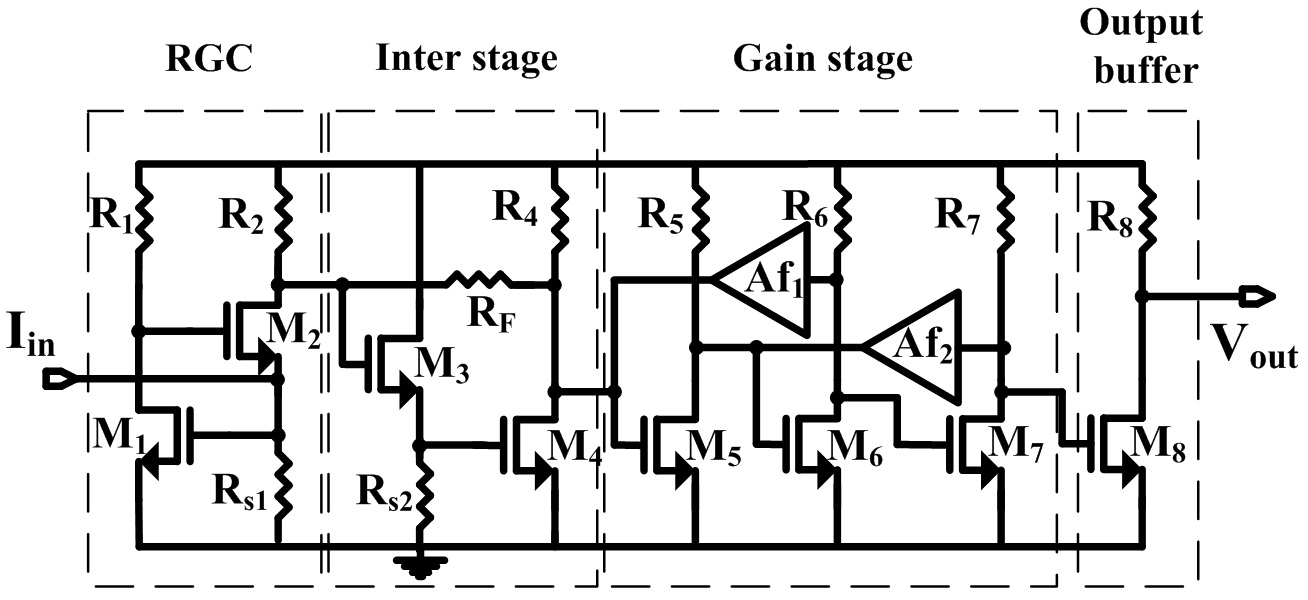
The schematic of the TIA-Rx chip is shown in Fig. 1. The RGC input stage reduces the input impedance by the amount of its own voltage gain, which prevents the input pole from dominating the TIA-Rx bandwidth and reduces the capacitive effect of the PD [8]. Thus, the RGC circuit can be used effectively for CMOS integration as a front-end amplifier.
The input impedance of the RGC stage is given as [4]:
where 1 +
At low frequency, the open-loop transimpedance gain of the TIA-Rx is given as:
The TIA-Rx is made up of four stages, namely, an input stage (which consists of the RGC); an inter-stage; a gain stage with intercepting active feedbacks; and an output stage (which acts as the buffer). The RGC block is important in the TIA-Rx circuit as it affects the input noise and the stability of the whole TIA-Rx circuit while delivering the input photo current to the output with increased gain. Thus, the design parameters have to be carefully chosen not to interfere with the input impedance for high frequency operation. The transfer function of the RGC input stage is given as:
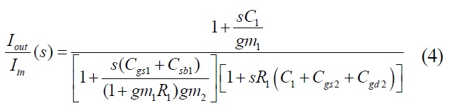
M3 and M4 make up the transconductance inter-stage stage of the TIA-Rx, where high frequency operation should be maintained for delivering the converted input current to output voltage for the gain stage. The impedance at the drain of M2 and M4 are reduced by factor of 1+
where
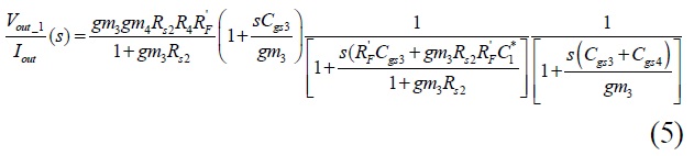
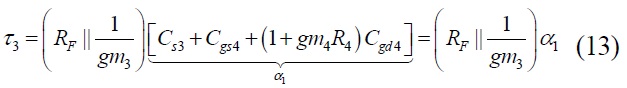
To increase the overall transconductance of the TIA-Rx to higher output voltage levels, several stages of commonsource (CS) amplifying stages have been utilized. However, placing a gain stage consisting of several CS amplifying stages may reduce the bandwidth. Hence, adding the active feedback stages, Af1 and Af2, compensate by peaking at high frequencies [9]. The negative active feedback utilized in the gain stage is different from the conventional resistive feedback which avoids the direct resistive load to the preceding transimpedance stage. Moreover, active devices suffer less process variation than passive devices during fabrication. The high-frequency peaking occurs at Af1 and Af2 active feedback. The peaking of the first and second active feedbacks is given as:
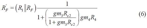
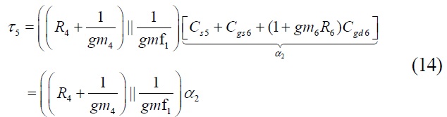
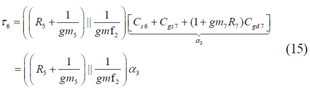
The negative active feedback increases the 3-dB bandwidth and thus, the active feedback effects of Af1 and Af2 has been included in the transfer function of the gain stage and the equation is given as:
where
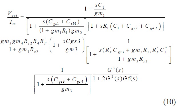
The transimpedance gain of the TIA-Rx can be obtained from equation (10) and is written as follows:
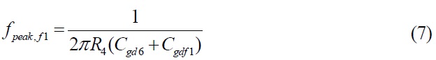
The 3-dB bandwidth of the TIA-Rx is affected by dominant poles at amplifying stages of

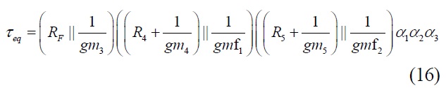
The 3-dB response of the TIA-Rx can be obtained with
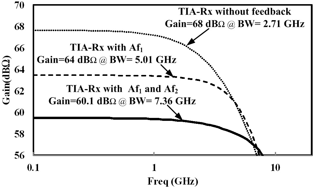
Figure 2 shows the transimpedance gain of the TIA and the bandwidth extension effect of the active feedbacks Af1 and Af2. The dotted line is the simulation result of TIA-Rx without active feedback which has a gain of 68 dBΩ at a 3-dB bandwidth of 2.71 Ghz; the dashed line is the result of TIA-Rx with active feedback, Af1, with 3-dB bandwidth of 5.01 GHz; and the solid line is the result of TIA-Rx gain with two feedbacks Af1 and Af2, where the transimpedance gain reduced to 60 dBΩ with a 3-dB bandwidth of 7.36 GHz. The 3-dB bandwidth has been improved from a value of 2.71 GHz to 7.36 GHz after adding two active feedbacks.
The input-referred noise of TIA-Rx can be described as follows:
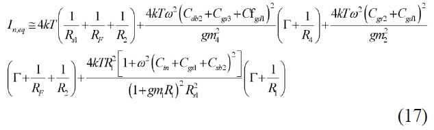
where
to be as large as possible, and to reduce the parasitic capacitance the transistors, M1, M2 and M3 sizes should be reduced. However, increasing
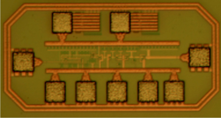
The proposed TIA-Rx circuit has been designed and fabricated in a 0.13 μm CMOS technology. The fabricated TIA-Rx chip core occupies an area of 0.051 mm2. The TIA-Rx chip is mounted on wire-bounded chip-on-board (COB) for frequency response, eye-diagram and integrated output noise measurements. The photograph of TIA-Rx chip is shown in Fig. 4.
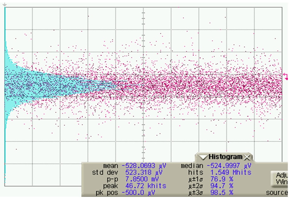
Figure 5 shows the integrated output noise measured from the output of the TIA-Rx chip with no input connected. The standard deviation of 0.52 mV is measured and by subtracting the oscilloscope noise of 0.1 mV, the corrected integrated noise is 0.42 mV.
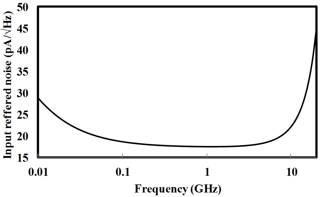
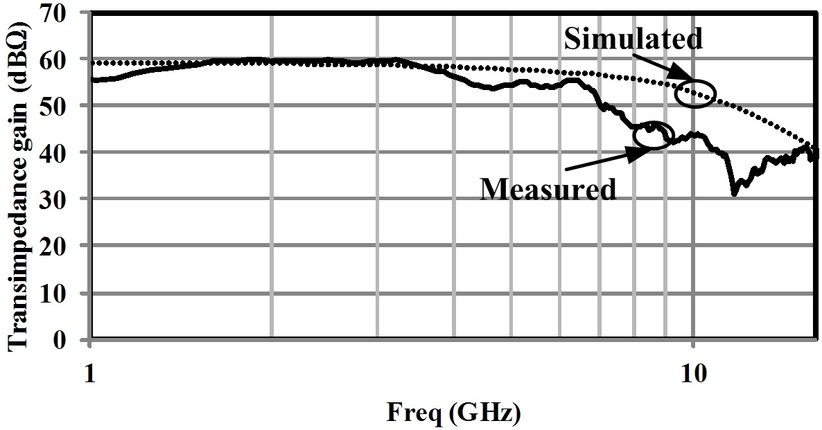
The frequency response is measured using an Agilent 8703B lightwave component analyzer. The measured 3-dB bandwidth of the TIA-Rx chip is 6.9 GHz and a transimpedance gain of 60 dBΩ, as shown in Fig. 6, which were obtained with 1 kΩ shunt passive feedback,
[TABLE 1.] The comparison of the proposed TIA-Rx chip performance with other works
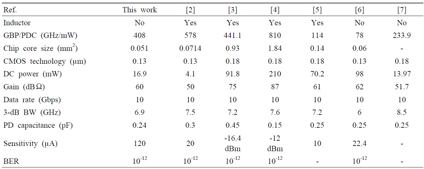
The comparison of the proposed TIA-Rx chip performance with other works
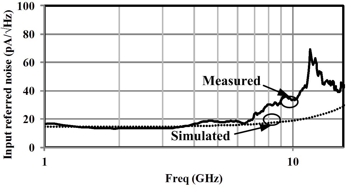
discrepancy between the measured and simulated results may have been attributed by process variation during the fabrication process.
Table 1 shows a comparison of the TIA-Rx performance with other works. From Table 1, it can be seen that the size of the proposed TIA-Rx is smaller than the other TIA circuits, where passive inductor peaking have been utilized for bandwidth extension. In our proposed TIA-Rx, using active feedback system achieves comparatively high gain-bandwidth product per DC power (GBP/PDC) figure of merit of 408 GHzΩ/mW with reduced chip area.
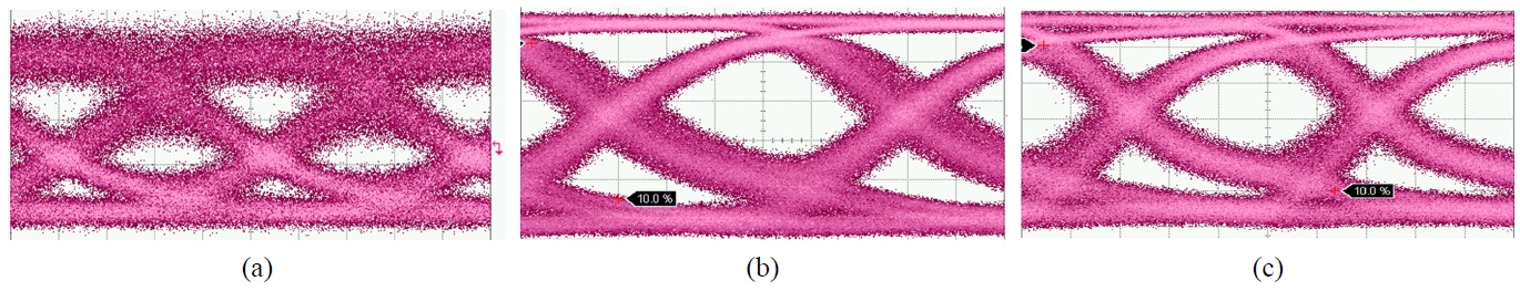
To evaluate optical TIA-Rx dynamic response, 231-1 pseudorandom binary sequence (PRBS) input signal, generated from Anritsu MP1736 pulse-pattern generator was applied, while the output was measured with an Agilent 8610A oscilloscope. The eye-diagrams of TIA-Rx are shown in Fig. 8. The applied input current 20 μA, 120 μA and 850 μA results in 20 mV, 120 mV and 750mV TIA-Rx output, respectively. The eye-diagrams of TIA-Rx show rise/fall times with root-mean square (RMS) jitter of 86.7/90ps with 13 ps for
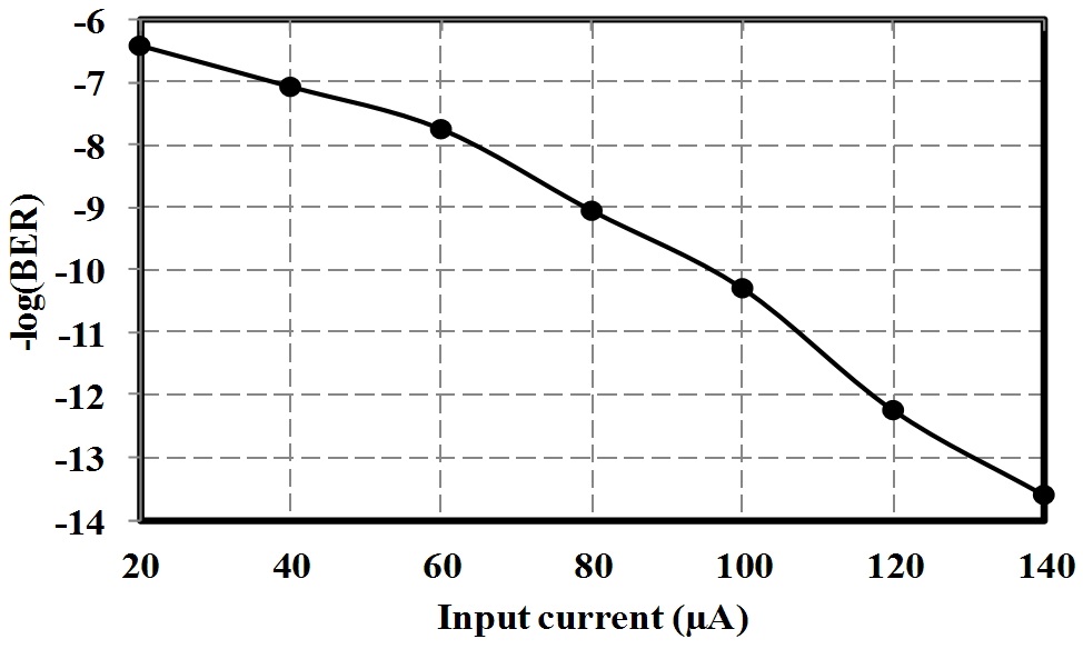
the input current is presented in Fig. 9. This BER measurement is done at 10 Gbps data rate using 231-1 PRBS input signal, and a BER of less than 10-12 is achieved with input current of about ~120 μA. The power dissipation of the TIA-Rx is 16.9 mW at 1.3 V.
Besides reducing input impedance of TIA-Rx, the RGC block with local (resistive) feedback increases the input referred noise as well. The addition of post amplifying transconductance stages adds extra noise. The increase in input-referred noise leads to degradation of input sensitivity. As a result, the dynamic characteristics (eye diagram) of the TIA-Rx chip shows better performance with slightly higher input current than the TIA-Rx with lower input current. From the eye-diagrams and BER measurement results are shown in Figs. 8 and Fig. 9, with increase of an input current, the output voltage of the TIA-Rx increases. Thus, our proposed TIA-Rx design requires higher input current of about ~120μA and above to be able to provide sufficient output signal to the next stages such as De-serializer, PLL, and clock data recovery (CDR) circuitry. Hence, our proposed TIA-Rx can be applied as a front-end optical Rx to convert the input photo current to the output voltage signal in order to feed to the De-serializer, PLL and CDR circuits.
A TIA-Rx has been designed and implemented in 0.13 μm CMOS technology for optical interconnect applications operating up to 10 Gbps. The TIA-Rx shows a good eye performance up to 10 Gbps with BER of less than 10-12. The TIA-Rx chip core is 0.051 mm2 with power consumption of 16.9 mW at 1.3 V. The measured input-referred noise of the TIA-Rx is 20pA/√Hz with a 3-dB BW of 6.9 GHz. The TIA-Rx chip utilizes two intersecting active feedback systems with RGC input stage and occupies a small chip area with an efficient GBP/PDC figure of merit of 408 GHzΩ/mW. Our proposed TIA-Rx can be applied as a front-end optical Rx to convert the input photo current to output voltage signal, high enough to feed to the next stages such as the De-serializer, PLL, and/or CDR circuits, and it is applicable for chip-to-chip optical interconnects.