Extreme ultraviolet lithography (EUVL) using a 13.5-nm wavelength light is expected to be employed as a nextgeneration technology because it has the potential to decrease the size of semiconductor devices to half-pitch of 16-nm and below [1]. However, it is reported that the lithography performance of an EUVL mask depends on the thickness of absorber materials because it is directly related to the imaging contrast, shadowing effect, focus shift effect, and thermal effect [2]. Therefore, the development of novel mask materials with high absorption at EUV is important for an actinic inspection of the mask and a high numerical aperture (NA) optical system [3]. Since a EUVL mask is a reflective type mask, it should have a high reflection contrast at 13.5-nm wavelength and also be thin enough to reduce the shadowing effect due to the oblique incidence of EUV light on the mask. Hence, the absorber material for the EUVL mask should have a high absorption coefficient at 13.5-nm wavelength. But, there is a discrepancy in microstructure and optical properties between the thin film and the corresponding bulk material. Therefore, the optical constant of thin films in the EUV region is measured directly. In the direct method, the EUV light source is a large and expensive facility. It would be convenient, if a new method, fast and indirect, could be used to determine the optical constants of thin films by using the techniques which are easily accessible in the laboratory.
The optical constants of materials in the extreme ultraviolet (EUV) wavelength region were determined by several authors. Windt
In this study, we propose a simple and indirect method to determine the optical constant of thin films in the EUV wavelength region by using X-ray reflectometry (XRR) and Rutherford backscattering spectrometry (RBS). The density and stoichiometry of the film are obtained by XRR and RBS, respectively, and these values are used to calculate the optical constants of Mo and ITO thin films at 13.5-nm wavelength.
II. DETERMINATION OF THE OPTICAL CONSTANTS
2.1. Optical Constant in the Extreme Ultraviolet Wavelength Region
In the EUV lithography, a 13.5-nm wavelength is used, which is large compared to the individual atomic size. The individual atoms, as dipoles, scatter independently in the EUV region. The total coherently scattered amplitude is the sum of the amplitude scattered around the individual atoms [8-9].
Then, the optical constant of a material in the EUV region is given by the well-known dispersion equation or macroscopic-to-atomic relationship [8-10]:
where
During the growth of a thin film by physical methods such as evaporation or sputtering, the vapor condensation onto a substrate leads to little crystals build up at numerous places with various crystallographic directions [11-12]. So there is considerable disagreement in the microstructure between the thin film and the corresponding bulk material. Therefore, the optical constant of the film is different from that of the bulk and the optical character of the thin film is inferior to the bulk.
In this study, the density and chemical composition of thin film is measured by XRR and RBS, respectively, and then the optical constant of thin film at 13.5-nm wavelength can be determined by Eq. (1) along with an assumption that the atomic scattering factor of film is the same as that of the bulk in the Henke
2.2. X-ray Reflectometry and Rutherford Backscattering Spectrometry
If a typical XRR radial scan is performed in a specular condition, the XRR curve can be obtained by plotting the scattered X-ray intensity against the angle of incidence [13]. Since the refractive index of a solid medium is lower than the refractive index of the air in the X-ray energy region, an incident X-ray in the air can be totally externally reflected by the medium at low incident angles. Due to the total external reflection (TER) at low incidence angles the scattered intensity is to a first approximation constant and determines a plateau. The incidence angle beyond which total external reflection is cut off is referred to as the critical angle of total external reflection. In the X-ray region, the critical angle is dependent on the density of the material.
If the incident angle is greater than the critical angle at TER, the waves reflected from the upper and lower interfaces of a layer interfere and the intensity maxima and minima, i.e., interference fringes, appear in the XRR angular spectrum. The critical angle, fringe amplitude, fringe separation distance and envelope of the reflectivity spectrum depend on thin film properties such as density, layer thickness and roughness. So X-ray reflectometry can provide information on film thickness, mass density and interfacial roughness by fitting a theoretical reflectance to the measured one [13-17].
Rutherford backscattering spectrometry (RBS) is a wellestablished technique to characterize the chemical composition of a thin film. As the high energy He+ particles are incident on the sample, they are elastically scattered by nuclei in the sample. The nuclei in the sample are detected by counting the scattered helium ions as a function of energy. The higher the mass of an atom that is hit by a helium ion, the higher the energy of the ion will be after backscattering. Most of the helium ions will travel through the sample rather than backscattering, and during the travel the ions lose energy by interaction with the electron clouds around the target atoms. This energy loss introduces a depth scale in the RBS spectrum. An ion that is scattered at some depth loses additional energy on the way in and out of the target atom. Hence, the number of atoms of each element present in the sample can be determined [18-20].
Mo and ITO films were deposited in an RF magnetron sputtering chamber with 2 inch-diameter Mo and ITO targets, respectively. Si wafers were employed as substrates for structural and chemical analysis. Before deposition, the chamber was evacuated to a base pressure of ~1×10⁻⁶ Torr. The working pressure was maintained at 5.6×10⁻³ Torr during the film deposition. An Ar gas was used as a sputtering gas to deposit the films and O2 was admitted for ITO film deposition with an RF power density of 1.48 W/cm2.
X-ray reflectivity (XRR) is measured at an accelerated voltage of 40 kV and current of 20 mA and the wavelength of CuK
Rutherford backscattering spectrometry (RBS) (X-Rump, Computer Graphic Service) is employed for measurement of elemental composition of the film. RBS is measured with 2 MeV He+ at normal incidence, detection angle θ of 10° and integrated charge (dose) of 10μC. RUMP simulation software was used for chemical analysis of the thin films [19].
4.1.1. Mo thick film
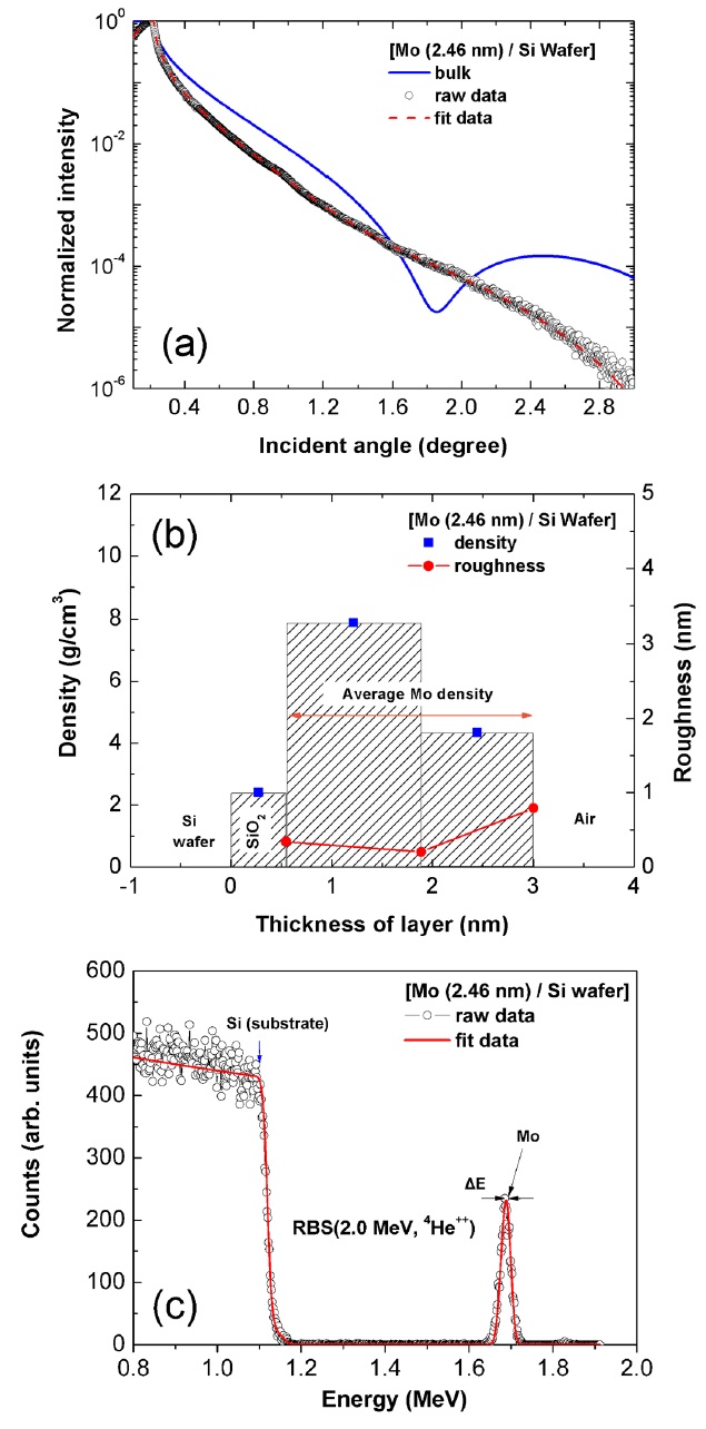
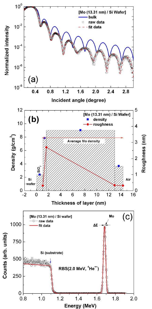
Figure 1(a) shows the measured XRR angular spectrum of Mo film with 13.31-nm thickness on a Si wafer. Also, the spectrum of Mo film of 13.31-nm thickness with zero roughness at bulk Mo density (10.2 g/cm3) is shown as a reference. The observed low peak intensity of the deposited Mo film compared to that of the film with bulk Mo density suggests that there is a surface and interface roughness in the Mo film. In addition, the irregular fringes between 1º and 1.8º indicate that the Mo film is inhomogeneous in density. Therefore, an inhomogeneous model is employed to simulate the XRR spectrum and the parameters such as density, thickness and roughness at surface and interfaces were evaluated by dividing the Mo film into inhomogeneous sublayers.
Figure 1(b) shows the density and roughness distribution of the Mo film with 13.31-nm thickness. In the simulation, a SiO2 layer of density 2.407 g/cm3 with 1.04 nm thickness is assumed to be on the Si substrate due to the surface oxidation. The Mo film can be modeled as a three-layer system on the top of the SiO2 layer. The first Mo thin layer starts to grow at a low density of 7.852 g/cm3 with 0.58-nm thickness, the second layer grows denser at a density of 9.023 g/cm3 with 11.33-nm thickness, and the third thin layer of 1.36-nm thickness becomes very porous with density of 3.685 g/cm3 due to the surface oxidation at the film-air interface. The mean density of the Mo film with 13.31-nm thickness is 7.939 g/cm3, which is much smaller than the bulk density of Mo, 10.22 g/cm3. In the three-layer inhomogeneous Mo film, the roughness between first and second layers is 2.694-nm, second and third
layers 0.337-nm and third layer and air interface 0.311-nm. It is noted that the three-layer inhomogeneous model in Fig. 1(b) is in good agreement with the measured XRR spectrum as shown in Fig. 1(a).
Stoichiometry of the Mo film is measured by RBS. Fig. 1(c) shows the measured and simulated RBS spectrum of Mo film with 13.31-nm thickness on the Si substrate. In the spectrum, Mo peak intensity is high compared to the O peak, which is very small and can be neglected. The composition of the Mo film was found to be MoO0.05, indicating that the film is composed of only Mo except for oxygen at the surface of the film.
The optical constants of the Mo film at 13.5-nm wavelength were calculated by substituting the mean density (7.94 gm/cm3) of the inhomogeneous Mo film from Fig. 1(b), the composition (MoO0.05) and the atomic scattering factor of Mo and O from Ref [7] into Eq. (1). The obtained optical constants of the Mo film are
4.1.2. Mo thin film
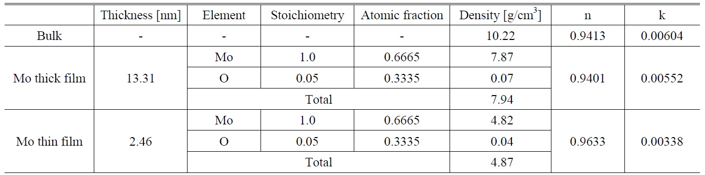
In the previous section, the first and third thin Mo layers have a lower density than the middle layer. Hence, we were interested in a similar analysis applied to a very thin Mo film with 2.46-nm thickness. An XRR angular spectrum of Mo film with 2.46-nm thickness on a Si wafer deposited by magnetron sputtering is shown in Fig. 2(a). In addition, the XRR spectrum of a Mo film with 2.46-nm thickness at bulk Mo density (10.2 g/cm3) is included in Fig. 2(a) for comparison. The first interference valley and peak are observed for the Mo film with bulk density at the angles 1.85º and 2.5º, respectively, while there are no interference fringes in the deposited thin Mo film spectrum.
A two-layer inhomogeneous model is employed to simulate the measured XRR spectrum of thin Mo film with 2.46-nm thickness. Fig. 2(b) shows that the density of the first layer with 1.34-nm thickness is 7.881 g/cm3 and the second layer with 1.12-nm thickness is quite porous with density of 4.329 g/cm3. It is noted that the two-layer model in Fig. 2(b) is similar to the first and third layers of the three-layer model in Fig. 1(a). The mean density of Mo thin film with 2.46-nm thickness is 4.87 g/cm3, which is much lower than that of the Mo film with 13.31-nm thickness. The roughnesses of the first layer and the second layer are 0.341 and 0.792-nm, respectively.
Figure 2(c) shows the RBS spectrum of Mo thin film with 2.46-nm thickness on Si substrate and the simulated data also included in the spectrum. The composition of the Mo thin film is MoO0.05. The optical constants of Mo thin film with 2.64-nm thickness at 13.5-nm wavelength were calculated as
[TABLE 1.] The density, stoichiometry and optical constant of bulk Mo and films

The density, stoichiometry and optical constant of bulk Mo and films
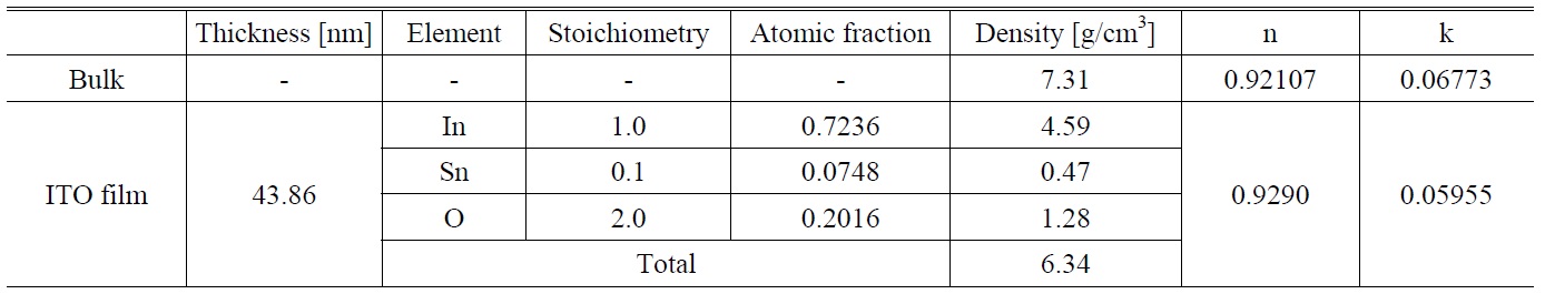
[TABLE 2.] The density, stoichiometry and optical constant of bulk ITO and films

The density, stoichiometry and optical constant of bulk ITO and films
index is larger and the extinction coefficient is smaller than those of the bulk Mo, indicating that the 2.46-nm thickness Mo film would show more a dielectric-like optical property than the bulk Mo.
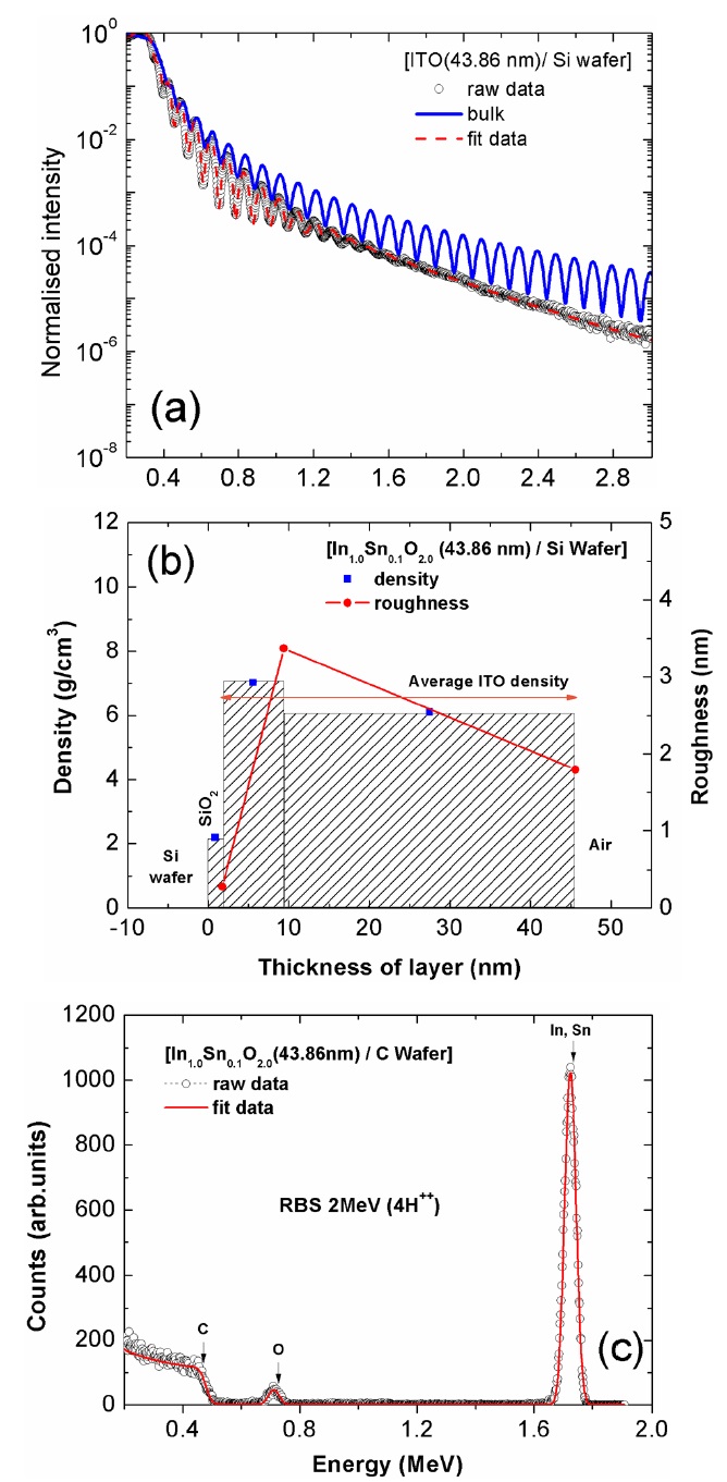
Figure 3(a) shows the measured and simulated XRR spectrum of the deposited ITO film with 43.87-nm thickness on a Si wafer. The thickness of the ITO film around 40-nm is chosen in the present work due to its smaller shadow effect. An XRR spectrum of the ITO film with bulk density (7.31 gm/cm3) is also included in Fig. 3(a) for comparison. The XRR spectrum of the deposited ITO film shows the progressive damping of interference fringes due to the large interface roughness. The two-layer model is employed to simulate the XRR spectrum as shown in Fig. 3(b). The density of the first layer is 7.029 g/cm3 with 7.62-nm thickness and that of the second layer 6.114 g/cm3 with 36.23-nm thickness. The mean density of ITO film with 43.86-nm thickness is 6.572 g/cm3. The roughnesses of the first and second layer are 3.371 and 1.795-nm, respectively.
Figure 3(c) shows the RBS spectrum of the ITO film with 43.86-nm thickness. The composition of the ITO film is evaluated as InSn0.1O1.6 from the simulated RBS spectrum in Fig. 3(c). It is a typical compound of 90% of In2O3 and 10% of SnO2. Table 2 gives the stoichiometry, density and atomic fraction of each element. The optical constants of ITO film with 43.86-nm thickness were calculated by substituting the average film density and the atomic scattering factor of each element in Eq. (1). The calculated optical constants of ITO film are
In this paper, we employed a simple and indirect method to determine the optical constants of Mo and ITO thin films at 13.5-nm wavelength by using X-ray reflectivity (XRR) and Rutherford backscattering spectrometry (RBS). The optical constants of Mo film with 2.46-nm thickness were calculated as n = 0.9633 and k = 0.00338 at 13.5-nm wavelength. Similarly, the optical constants of ITO film with 43.86-nm thickness were n = 0.9290 and k = 0.05955 at 13.5-nm wavelength. In both Mo and ITO film, the optical constants were different from the corresponding bulk values. In summary, the XRR and RBS techniques were used as a fast method for determination of the optical constants of thin films in the EUV region in place of the expensive direct method.