Zinc oxide (ZnO) is a wide-band gap II-VI semiconductor, and ZnO films have potential applications as surface acoustic wave devices (SAW) [1], low loss optical wave-guides [2] and transparent conducting oxide (TCO) electrodes [3,4]. The growth of ZnO thin films has been investigated by several techniques such as atomic layer deposition [5], radio frequency magnetron sputtering [1] and pulsed laser deposition [6].
In this study, radio frequency (RF) magnetron sputtering and electron irradiation technology were used to prepare ZnO thin films on glass substrates, and the effect of electron irradiation energy on the structural, electrical and optical emission properties of ZnO films was investigated.
The sputter chamber was evacuated to 1×10⁻⁴ Pa, and ZnO thin films were deposited in a pure Ar/O2 gas mixture on a glass substrate (size: 5×5 cm2) with RF magnetron sputtering. Prior to being placed on the holder, the substrate was cleaned in acetone and methanol, rinsed in de-ionized water, and dried in flowing nitrogen gas. A ceramic ZnO target (99.99% purity, 3 in. diameter) was used. The surface of the film was irradiated by an intense electron beam for 30 minutes. The thicknesses of the films were maintained at 100 nm by controlling the deposition time. The distance between the target and substrate was maintained at 6 cm for all depositions. After deposition, the crystallinity was measured with an X-ray diffractometer (XRD, Cu-Kα X’pert Pro MRD, Philips). The variation in grain size was obtained as a function of electron irradiation energy using the Scherrer formula [7], and the optical emission properties of the films were characterized by Photoluminescence (PL, Lan Ram HR, Sci-Tech Instruments, Korea Basic Science Institute, Sunchon Center). In addition, the optical transmittance in the visible region was measured with a UV-Vis. spectrophotometer (Cary 100 Cone, Varian).
[Table 1.] The deposition parameters and conditions for the ZnO thin films.
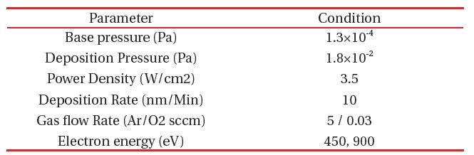
The deposition parameters and conditions for the ZnO thin films.
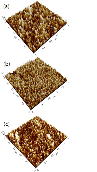
Surface morphology and root mean square (RMS) roughness of the irradiated films were also observed under different electron energies by atomic force microscopy (AFM) at atmospheric pressure.
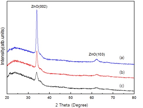
Structural characterization is important for explaining the optical and electrical properties of ZnO films. Figure 1 shows the XRD patterns of the films. The diffraction peaks in the pattern were identified as ZnO (002) and (103) planes of the ZnO Wurtzite structure and the peak intensity of the ZnO (002) decreased proportionally with electron irradiation energy.
In XRD patterns, the full widths at half maximum (FWHM) for the 2θ values revealed the crystallinity of the films and grain size evaluated by the Scherrer formula [7]. Prior to electron irradiation, as deposited ZnO films showed a grain size of 10.6 nm, while electron irradiated films at 450 eV and 900 eV show decreased grain sizes of 10.2 and 6.7 nm, respectively.
From the XRD pattern, we concluded that the increase in electron irradiation energy deteriorates the crystallinity of the film. In a previous study, intense negative ion beams for ITO deposition also showed similar results, in that the grain sizes of the ITO films decreased inversely with negative ion beam energy [8].
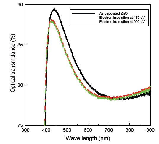
Figure 2 shows the optical transmittances of ZnO films in the UV-visible region. The transmittance of thin film depends on crystallinity, because the grain boundary may absorb visible light, resulting in low optical transmittance [9]. In this study, asdeposited ZnO films show higher transmittance of 82% than those of the electron irradiated films. The electron irradiated films at 450 eV show a transmittance of 81% and the films irradiated at 900 eV show the lowest optical transmittance of 80%.
Based on XRD patterns, the decrease in optical transmittance in the visible region by intense electron irradiation is attributed to the decreased grain sizes of the films.
Figure 3 shows an AFM image and RMS roughness obtained from as-deposited films and ZnO films electron irradiated at 450 eV and 900 eV, respectively. As- deposited ZnO films show the higher RMS roughness of 2.3 nm and the electron irradiated films at 450 eV show RMS roughness of 2.0 nm. The lowest RMS roughness of 1.6 nm was observed at ZnO films electron irradiated at 900 eV. From the XRD patterns and AFM images it can be concluded that the intense electron irradiation promotes the flatness of surface morphology and decreases the grain size of the films.
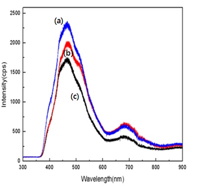
Figure 4 shows the photoluminescence of ZnO films electron irradiated with different electron bombarding energies. UV PL characteristics of ZnO films were strongly related to the electron energy. For as-deposited ZnO films, Zn and O2 molecules did not have enough energy to form stoichiometric ZnO films. As the electron energy increased to 900 eV, the intensity of UV emission increased. This result indicates that the ZnO films irradiated with electrons at 900 eV are more stoichiometric than films irradiated at 450 eV. In a previous study, the stoichiometric of the ZnO films
grown by pulsed laser deposition (PLD) was improved by increasing the substrate temperature [10]. Thus, the stoichiometric of the ZnO films was improved by increasing the electron irradiation energy.
Highly C-axis oriented ZnO films were prepared on glass substrate by RF magnetron sputtering and post deposition via an electron irradiation technique. The ZnO film irradiated at 900 eV showed the highest UV PL intensity.
Since the intensity of UV emission is dependent upon the stoichiometric of ZnO films, we found that an electron energy of 900 eV was the optimum irradiation energy to achieve the best stoichiometric of ZnO thin films in this study.