ZnO is a versatile material that possesses a wide range of applications as active component in gas sensors, optical devices, grain boundary effect devices, etc. ZnO varistors are typical semiconducting electro-ceramic devices, which exhibit a nonlinear V-I relation due to the grain boundary effect formed by sintering ZnO powder with minor additives [1]. The sintering process gives rise to a microstructure, which consists of semiconducting n-type ZnO grains surrounded by very thin insulating intergranular layers. Each ZnO grain acts as if it has a semiconductor junction at the grain boundary [2,3]. Since nonlinear electrical behavior occurs like back-to-back zener diode at each boundary, the impurity doped ZnO varistors can be considered as a multi-junction device composed of many series and parallel connection of grain boundaries [2,3]. The grain size distribution plays a major role in electrical behavior. Electrically, ZnO varistors exhibit highly nonlinear voltage-current (V-I) properties expressed by the relation I = CVα, where I is the current, V is the voltage, C is a constant, α is the nonlinear coefficient, which characterizes the nonlinear properties of the varistors [4,5].
ZnO ceramics cannot exhibit a varistor behavior without adding heavy elements with large ionic radii such as Bi, Pr, Ba, etc. Commercial ZnO-Bi2O3-based ceramics and ZnO-Pr6O11-based ceramics cannot be co-fired with a silver inner-electrode (m.p. 961℃) in multilayered chip varistors because of the relatively high sintering temperature above 1,000℃ [6,7]. Therefore, new varistor ceramics are required in order to use a silver innerelectrode. Among the various ceramics, one candidate is the ZnO-V2O5 ceramics [8,9]. This system can be sintered at a relatively low temperature in the vicinity of about 900℃. This is very important for multilayered chip varistor applications, because it can be co-sintered with a silver inner-electrode without using expensive palladium or platinum metals [8,9].
A study on ZnO-V2O5-based ceramics is in early stage in terms of ceramic composition and sintering process [10-18]. To develop useful ZnO-V2O5-based ceramics, as usual it is very important to investigate the effects of various additives on varistor properties. In this paper, the effects of additives (Cr, Nb, Dy, and Bi) on varistor properties and aging behavior of ZnO-V2O5-MnO2-Co3O4-La2O3 (ZVMCL) ceramics were systematically examined and new results were attained.
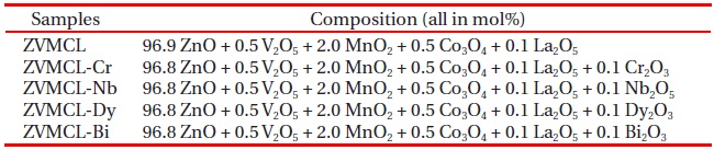
Reagent-grade raw materials were prepared in the proportion of ZVMCL [96.9 mol% ZnO + 0.5 mol% V2O5 + 2.0 mol% MnO2 + 0.5 mol% Co3O4 + 0.1 mol% La2O3]+ (0.1 mol% Cr2O3, 0.1 mol% Nb2O5, 0.1 mol% Dy2O3, and 0.1 mol% Bi2O3, independent additives added to ZVMCL composition). The detailed composition of the samples is shown in Table 1. Raw materials were mixed by ball milling with zirconia balls and acetone in a polypropylene bottle for 24 h. The mixture was dried at 120℃ for 12 h. The dried mixture was mixed by a magnetic stir bar into a container with acetone and 0.8wt% polyvinyl butyral (PVB) binder of powder weight. After drying at 120℃ for 24 h, the mixture was granulated by sieving through a 100-mesh screen to produce starting powder. The powder was uniaxially pressed into disk-shaped pellets of 10 mm in diameter and 1.3 mm in thickness at a pressure of 100 MPa. The pellets were sintered at 900℃ in air for 3 h and furnace cooled to room temperature. The final pellets were about 8 mm in diameter and 1.0 mm in thickness. Conductive silver paste was coated on both faces of the pellets and the electrodes were formed by heating it at 550℃ for 10 min. The electrodes were 5 mm in diameter. Finally, after soldering the lead wire to both electrodes, the samples were packaged by dipping them into a thermoplastic resin powder.
2.2 Microstructure examination
Both surfaces of the samples were lapped and ground with SiC paper and polished with 0.3 μm-Al2O3 powder to a mirrorlike surface. The polished samples were chemically etched into 1 HClO4:1000 H2O for 25 s at 25℃. The surface of the samples was metallized with a thin coating of Au to reduce charging effects and to improve the resolution of the image. The microstructure was examined by a scanning electron microscope (SEM, Hitachi S2400, Chiyoda-Ku, Tokyo, Japan). The average grain size (d) was determined by the lineal intercept method such as the expression, d = 1.56 L/MN [19], where L is the random line length on the micrograph, M is the magnification of the micrograph, and N is the number of the grain boundaries intercepted by the lines. The crystalline phases were identified by an X-ray diffractometer (XRD, X'pert-PRO MPD, the Netherlands) with Ni filtered CuKα radiation. The sintered density (ρ) of pellet was measured using a density determination kit (238490) attached to a balance (AG 245, Mettler Toledo International Inc., Greifensee, Switzerland).
The electric field-current density (E-J) characteristics were measured using a high voltage source unit (Keithley 237, Keithley Instruments Inc., Cleveland, OH, USA). The breakdown field (E1 mA)
[Table 1.] Composition of the samples.

Composition of the samples.
was measured at 1.0 mA/cm2 and the leakage current density (JL) was measured at 0.8 E1 mA. In addition, the nonlinear coefficient (α) is defined by the empirical law, J = C·Eα, where J is the current density, E is the applied electric field, and C is a constant. The α was calculated by the following expression, α = 1/(logE2-logE1), where E1 and E2 are the electric fields corresponding to 1.0 mA/cm2 and 10 mA/cm2, respectively.
The dielectric characteristics, such as the apparent dielectric constant (εAPP') and dissipation factor (tanδ) were measured in the range of 100 Hz to 2 MHz using an RLC meter (QuadTech 7600, Marlborough, MA, USA).
2.5 DC accelerated aging characteristic measurement
The DC accelerated aging test was performed for stress state of 0.85 E1 mA/85℃/24 h. Simultaneously, the leakage current was monitored at intervals of 1 min during stressing using a high voltage source unit (Keithley 237). The degradation rate coefficient (KT) was calculated by the expression IL = ILo + KT t1/2 [20], where IL is the leakage current at stress time (t) and ILo is IL at t = 0. After applying the stress, the E-J characteristics were measured at room temperature.
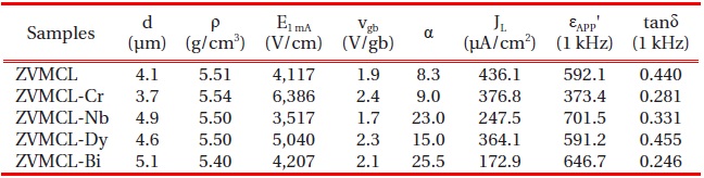
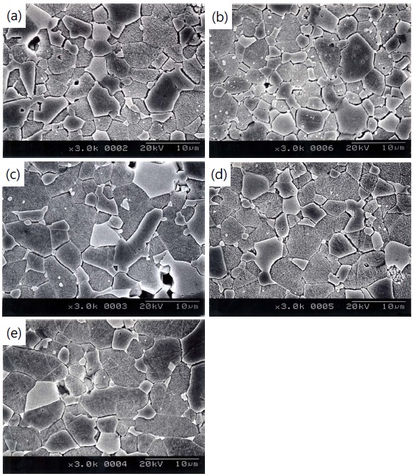
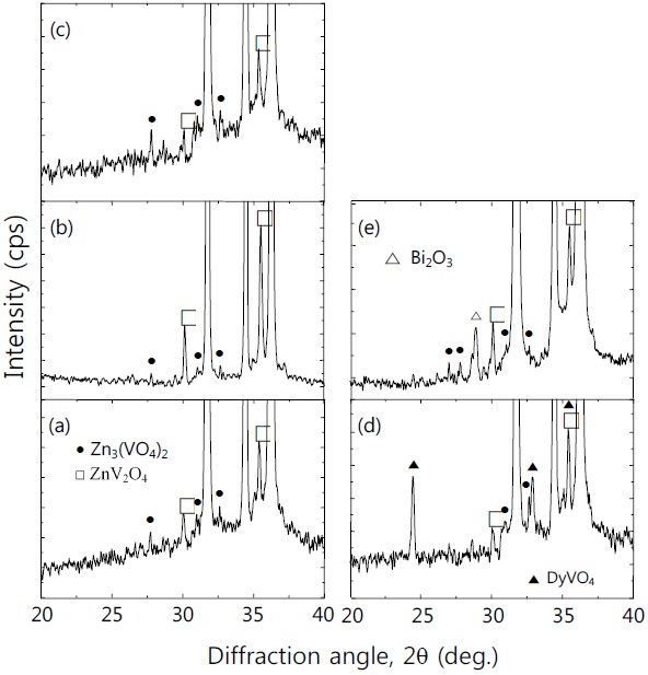
Figure 1 shows the SEM micrographs of surface of the samples for different additives. The grain structure is relatively homogeneously distributed throughout the entire samples, compared with ternary ZnO-V2O5-MnO2 ceramics [13]. The average grain size (d) decreased in the order of ZVMCL-Bi (5.1 μm) > ZVMCL-Nb (4.9 μm) > ZVMCL-Dy (4.6 μm) > ZVMCL (4.1 μm) > ZVMCL-Cr (3.8 μm). It was found that the additives such as Bi, Nb, and Dy improved the grain growth, whereas the Cr inhibited it. The grain growth in the samples doped Bi and Dy is attributed to liquid phase Bi2O3 and DyVO4, respectively. On the other hand, the additive such as Nb seems to prompt the movement of the grain boundaries because of the increase of interface energy at the grain boundaries. On the contrary, the additive such as Cr seem to hinder the movement of the grain boundaries because of the decrease of interface energy at the grain boundaries. The sintered density (ρ) was 5.51 g/cm3 for the ZVMCL, 5.54 g/cm3 for the ZVMCL-Cr, 5.50 g/cm3 for the ZVMCL-Nb and ZVMCL-Dy, and 5.40 g/cm3 for the ZVMCL-Bi. It is presumed that the low sintered density of the ZVMCL-Bi is attributed to the larger ionic radius of Bi than Zn ion. The detailed sintered density and average grain size of the samples are indicated in Table 2. The XRD patterns of the samples are shown in Fig. 2. All the samples revealed the presence of the secondary phase such as Zn3(VO4)2 and ZnV2O4. The secondary phases are formed when the ZnOV2O5- based ceramics are sintered at high temperatures and that acts as a liquid-phase sintering aid [8].
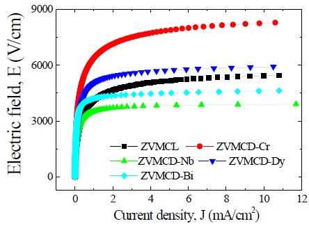
Figure 3 shows the electric field-current density (E-J) characteristics

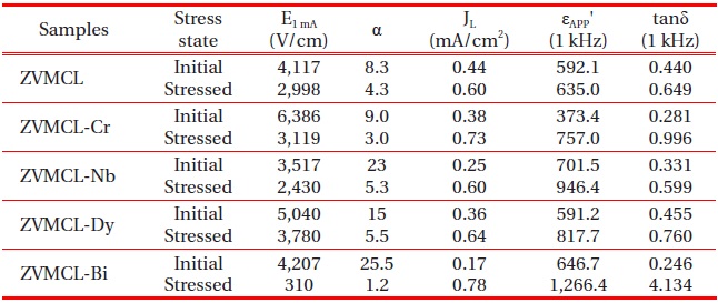
Microstructure, E-J, and dielectric characteristic parameters of the samples for different additives.
of the samples for different additives. The varistor properties are characterized by nonlinearity in the E-J characteristics. The conduction characteristics consisted of a linear region before breakdown and a nonlinear region after breakdown. The sharper knee of the curves between the two regions leads to the better nonlinear properties. It can be forecasted that the ZVMCL-Nb and ZVMCL-Bi should exhibit the good nonlinear properties in the light of the sharp knee. Therefore, it is clear that the additives such as Nb and Bi seem to significantly enhance the varistor properties. The breakdown field (E1 mA) decreased in the order of ZVMCL-Cr (6,386 V/cm) > ZVMCL-Dy (5,040 V/cm) > ZVMCL-Bi (4,207 V/cm) > ZVMCL (4,117 V/cm) > ZVMCL-Nb (3,517 V/cm). The E1 mA can be explained by both the average ZnO grain size and the breakdown voltage per grain boundaries (vgb), as expressed by the following expression [4]; E1 mA = vgb/d, where d is the grain size and vgb stands for the breakdown voltage per grain boundaries. In general, the decrease of the grain size leads to increasing E1 mA. However, the E1 mA decreases in the case of decrease of vgb though the d decreases. The all additives enhanced the nonlinear properties, in particular, the additives such as Nb and Bi significantly enhanced the nonlinear coefficient (α) beyond 20. The α decreased in the order of ZVMCL-Bi (25.5) > ZVMCL-Nb (23.0) > ZVMCL-Dy (15.0) > ZVMCL-Cr (9.0) > ZVMCL (8.3). It can be seen that each additive has a significant effect on the nonlinear properties. This is attributed to the barrier height caused by the electronic states at active grain boundary. The leakage current (IL) shows an opposite relation to the nonlinear coefficient (α). On the whole, the IL value is much higher than the expected value in the light of α value. Presumably, a high leakage current of these samples seems to be due to the recombination of electron and hole rather than thermionic emission over barrier at the grain boundary.
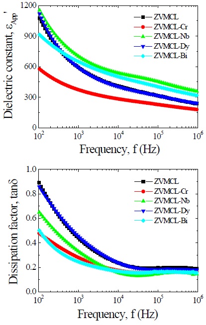
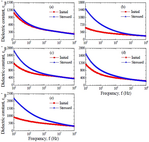
Figure 4 shows the apparent dielectric constant (εAPP') and dissipation factor (tanδ) of the samples for different additives. With increasing frequency for all samples, the εAPP' decreased with a relatively sharp dispersive drop less than 1 kHz. The εAPP' at 1 kHz decreased in the order of ZVMCL-Nb (701.5) > ZVMCL-Bi (646.7) > ZVMCL (592.1) > ZVMCL-Dy (591.2) > ZVMCL-Cr (373.4) and this tendency was maintained for the frequency above 1 kHz. This is directly related to d/t ratio, as can be seen in the following equation, εAPP' = εg(d/t), where εg is the dielectric constant of ZnO (8.5), d is the average grain size, and t is the depletion layer width of the both sides at the grain boundaries. On the other hand, the tanδ decreased until the vicinity of 20 kHz with increasing frequency, which exhibits very weak second dispersion peak in the vicinity of 300 kHz, and thereafter again decreased. The tanδ at 1 kHz decreased in the order of ZVMCL-Dy (0.455) > ZVMCL (0.440) >ZVMCL-Nb (0.331) (592.1) > ZVMCL-Cr (0.281) > ZVMCL-Bi (0.246). On the whole, the high tanδ coincides with a high leakage current. The tanδ might be attribute to the joule loss by the leakage current than frictional loss by dipole rotation. The detailed
dielectric characteristic parameters at 1 kHz are summarized in Table 2.
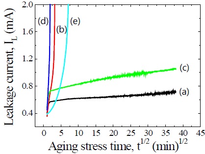
Figure 5 shows the variation of leakage current during DC accelerated aging stress of the samples for different additives. It can be seen that the additives have a significant effect on aging behavior. All the samples except for the ZVMCL and ZVMCL-Nb exhibited the thermal runaway within a short time (approximately 1 min) under specified DC accelerated aging stress of 0.85 E1 mA/85℃/24 h. The additives such as Cr, Dy, and Bi deteriorated the stability against an accelerated aging stress. In particular, the additive such as Bi improved nonlinear electrical properties, whereas it resulted in a severe problem in stability. On the contrary, the ZVMCL-Nb was found to exhibit a good stability without thermal run-away during specified stress time. The stability for nonlinear properties of the samples can be estimated by the degradation rate coefficient (KT), indicating the degree of aging from the slope of the IL-t1/2 curve. The lower the KT, the higher the stability. The KT value for sample ZVMCL exhibited +26.9 μA·h-1/2 and that for sample ZVMCL-Nb exhibited +62.6 μA·h-1/2.
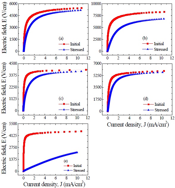
Figure 6 shows the E-J characteristic behavior after applying the stress for the respective samples. It can be seen that the variation of E-J curves after applying the stress is strongly affected by the additives. The ZVMCL, ZVMCL-Cr, and ZVMCL-Bi exhibited
E-J and dielectric characteristic parameters before and after applying the stress of the samples for different additives.
very large variation of E-J curves in the entire range of electric field after applying the stress. In particular, ZVMCL-Bi exhibited the ohmicity. On the contrary, the ZVMCL-Nb and ZVMCL-Dy exhibited a small variation in E-J curves after applying the stress, in particular, in the ZVMCL-Nb case. The detailed variation of E-J characteristic parameters after applying the stress is summarized in Table 3. ZVMCL, ZVMCL-Nb, and ZVMCL-Dy exhibited comparatively low variation within -30% in the %ΔE1 mA. Of the samples, ZVMCL-Dy exhibited the smallest variation despite the thermal runaway. It is assumed that this sample may be the result from quick recovery capability against a stress. Moreover, the %Δα of this sample is compared with ZVMCL and ZVMCLNb with no the thermal runaway. The ZVMCL and ZVMCL-Nb resulted in a large variation despite no the thermal runaway, contrary to expectation. Therefore, it is difficult to jump to a conclusion that the Nb is additives improving the stability against a DC stress for at least ZVMCL ceramics. On the other hand, it can be seen that the ZVMCL-Bi changed almost ohmic properties, as revealed in the % ΔE1 mA and %Δα.
Figure 7 shows the behavior of dielectric constant (εAPP') after applying the stress for the respective samples. The εAPP' of ZVMCL doped with impurities exhibited a large variation less than 100 kHz. The ZVMCL and ZVMCL-Cr, which revealed a thermal runaway, exhibited a high variation for εAPP'. However, the ZVMCL-Nb
and ZVMCL-Dy exhibited a comparatively low variation. This εAPP' behavior is very similar to E-J characteristic behavior. It is assumed that the reason why the εAPP' increases with DC stress is related to the migration of zinc interstitial (Zni) within depletion layer. The Zni is diffused toward grain boundaries under external stress and reacts with the negatively charged Zn vacancy:
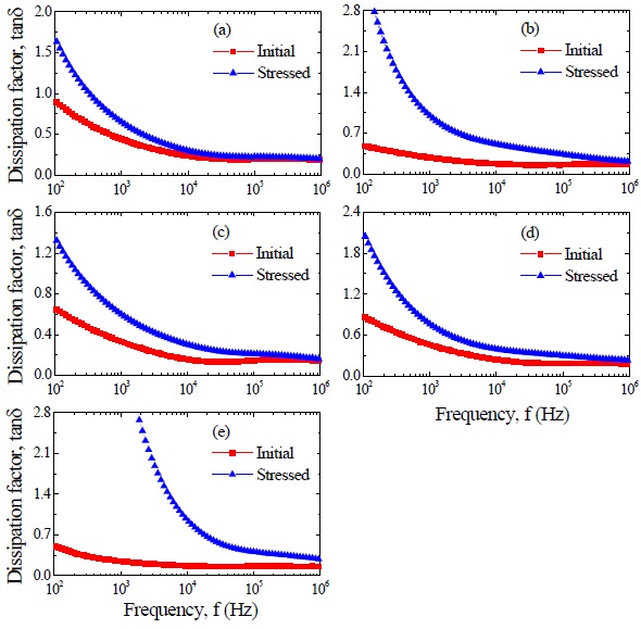
Figure 8 shows the behavior of dissipation factor (tanδ) after applying the stress for the respective samples. It can be seen that the tanδ also exhibited a similar behavior to the εAPP' after applying the stress. Other samples except for sample ZVMCL after applying the stress exhibited a very large variation more than %Δtanδ = 50%, in particular for ZVMCL-Cr and ZVMCL-Bi. Also, sample ZVMCL exhibited the high stability for tanδ, compared with other samples. It is assumed that the large variation rate of tanδ is attributed to the increase of leakage current in accordance with aging. The detailed variation of tanδ before and after applying the stress is summarized in Table 2. On the whole, the various additives in the ZVMCL ceramics deteriorated the stability in the dielectric characteristics, like the E-J characteristics.
In discussing stability, in general, macroscopically, the sintered density and the leakage current have a significant effect on the stability against a stress. That is, the higher the sintered density and the lower the leakage current, the higher the stability. The low sintered density decreases the number of parallel conduction path and eventually leads to the concentration of current. The high leakage current gradually increases the carrier generation due to Joule heat and it leads to repetition cycle between joule heating and leakage current. In this viewpoint, although the ZVMCL has a high leakage current, the ZVMCL did not exhibit any thermal run-away. On the contrary, although the ZVMCL-Bi has the lowest leakage current, it exhibited the thermal runaway. Therefore, it is difficult to assert that macroscopic factors such as sintered density and leakage current affect the stability. Microscopically, this is related to the rather migration of zinc interstitial (Zni) within depletion layer [21]. In this viewpoint, it
is guessed that the reason why the sample ZVMCL-Nb exhibits good stability is because the Nb spatially restricts the migration of ions within the depletion layer.
The electrical, dielectric properties, and aging behavior of ZnO-V2O5-MnO2-Co3O4-La2O3 (ZVMCL) ceramics were comprehensively investigated in accordance with different additives (Cr, Nb, Dy, and Bi). The phases formed for all the samples consisted of Zn3(VO4)2 and ZnV2O4 in common as the secondary phases in addition to ZnO grain as a main phase. The sintered density and average grain size were found to have a fluctuation in a reference for ZVMCL ceramics. All additives enhanced the varistor properties based on the nonlinear coefficient (α) and leakage current density. The ZVMCL ceramics modified with Bi and Nb exhibit a relatively high nonlinear coefficient, with α=25.5 and α=23, respectively. However, on the whole, all additives did not improve the stability against a DC stress, compared with ZVMCL ceramics. Conclusively, it was found that various additives have a significant effect on varistor properties of ZVMCL ceramics. Obviously, Nb and Bi will be significantly applied to as additives for ZnO-V2O5-based ceramics.