In the year 1954, the solar cell was firstly developed at Bell Laboratories in the United Stated [1], Over the past several decades, research for improving the power conversion efficiency of the solar cell has been progressing steadily. The strength of the generated electric field by the ionized carrier in the silicon junction with quantum mechanics is directly related to the output of the short-circuit current and open-circuit voltage of the solar cell. In addition, the symmetrical structure of positive and negative charge in the p-n junction structure is similar to the structure of the capacitance. The charge density increases and diffusion current distance is increased proportionally with capacitance volume. For the analysis by macroscopically with this associated theory, this study was scheduled.
Especially, silicon solar cell is commercialized in the most country of entire world. In the conjunction power conversion efficiency of the p-n junction silicon solar cell, this paper will be discussed intensively of electric field effect of changed capacitance of depletion region. To the increase research of power conversion efficiency of the silicon solar cell is very important of understanding of capacitance.
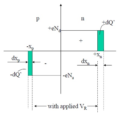
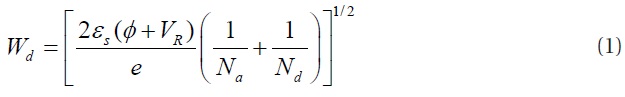
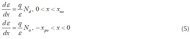
The charge generation is expressed as the sum of the transition region of the positive and negative charges and the position of the Fermi energy level with impurity doping concentration in the silicon p-n junction. The sum with the transition region of two surfaces is defined of depletion region. The following equation- 1 shows the depletion region length.
The formation of the transition is very similar to the electric field of capacitance region, it can be expressed as equation-2.
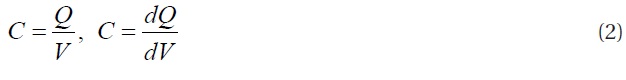
Equation-2 is calculated for capacitance volume along if cancellation voltage to charge parameter. Thus, capacitance will be changed to capacitance if applied to both charges of alternating current(AC) voltage with a frequency characteristic of each.
The charge density of this capacitor is directly related with the occurrence of short-circuit current of the silicon solar cell.
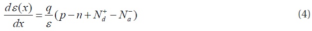
The electric field distribution of the charge density of the depletion region can be represented by a Poisson equation. The positive and negative charges can be expressed as follows: charge equation-3.

Each transition region can be expressed as follows from the space charge.
This current carrier is occurred diffusion effect by supplying energy to the excess carrier and electric field by sunlight absorption [2].
In the microscopic space charge region of the silicon p-n junction region, the occurrence source of the electric field by ionization carrier effect is very similar to the capacitor physical effect and if the capacitance volume increases, energy of the electric field increases also. This effect can be described in the charge density. Thus, changed electric field in the depletion region is analyzed through an experiment.
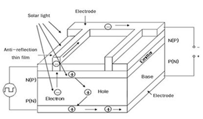
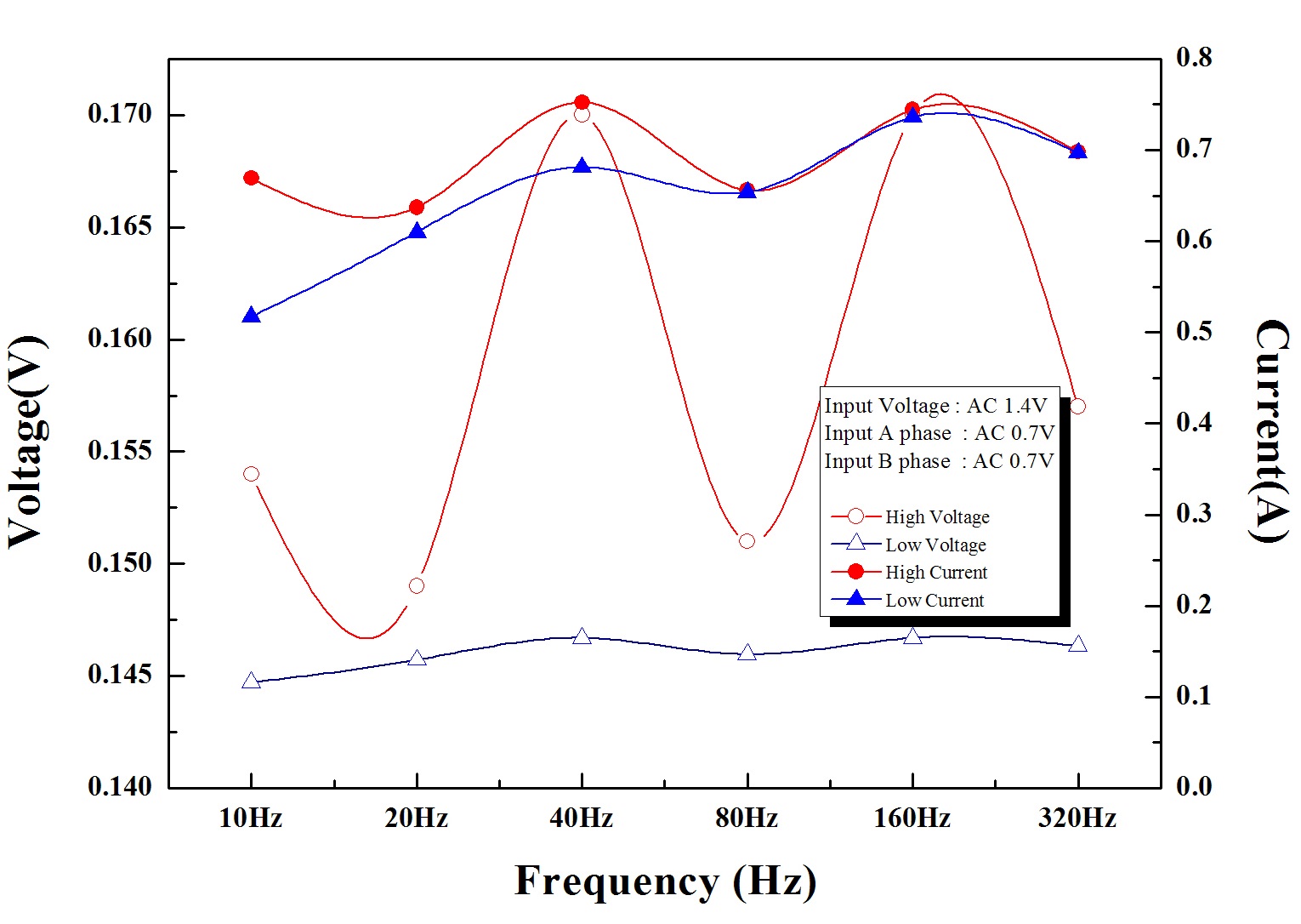
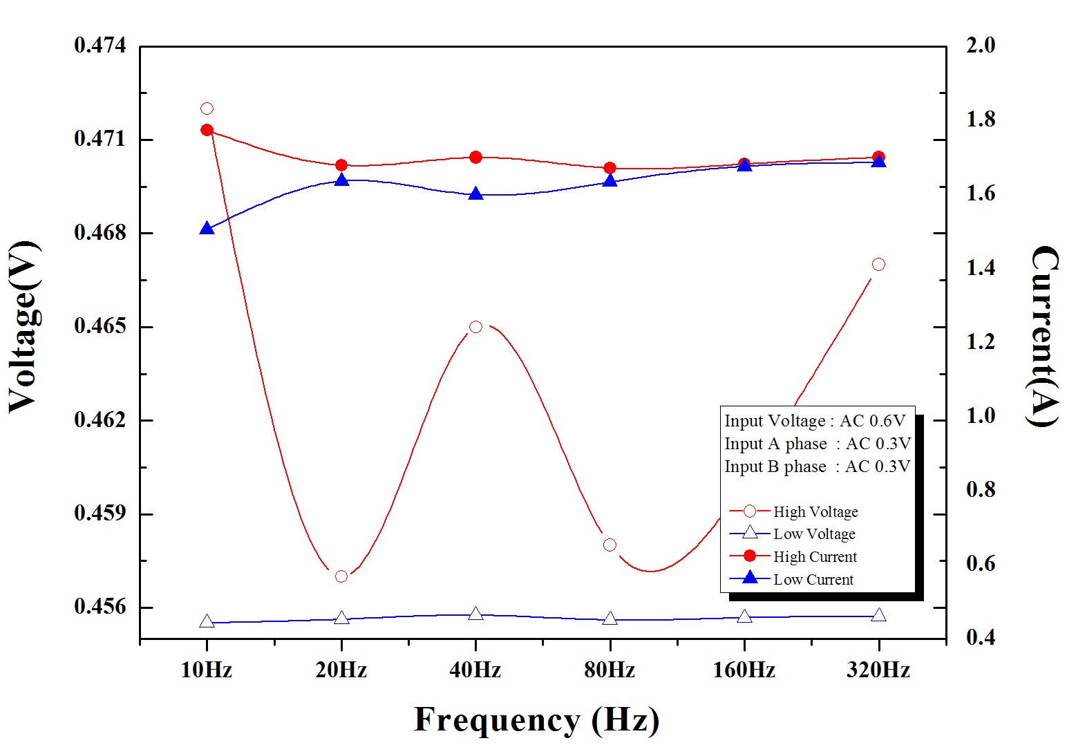
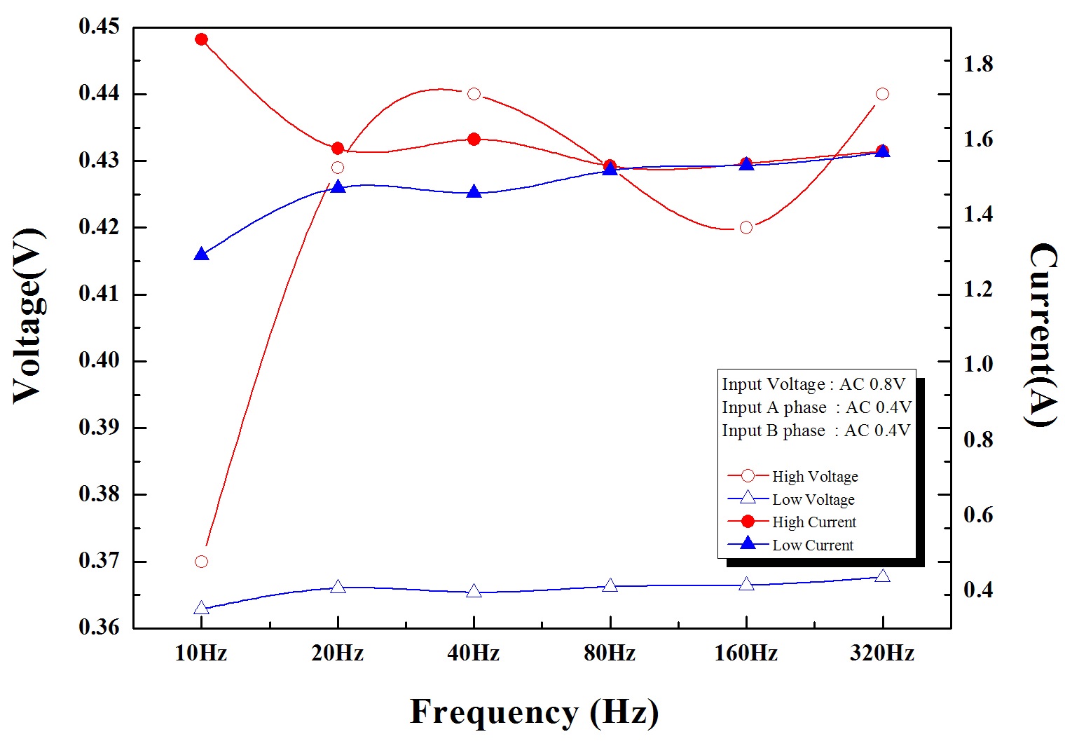
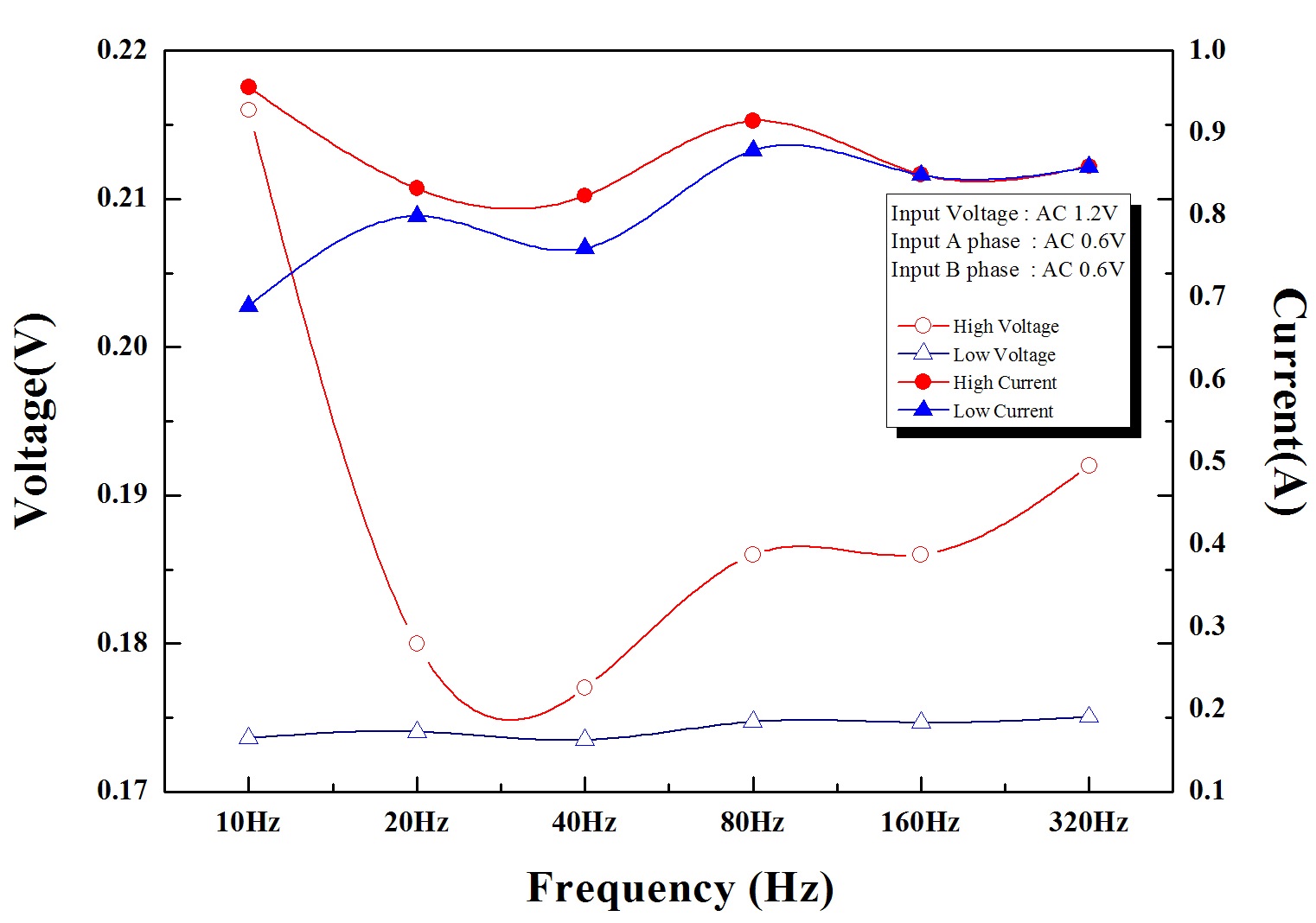
Figure 2. shows the experimental method of changed capacitance of the solar cell. In this experiment, 150 W halogen lamp light source (Solar cell and lamp distance : 5 cm, illumination : 110 000 lux) was used. The nature of the halogen lamp, light on of long time, due to occurrence of high temperature is generated. Thus, the measurement value of direct current(DC) voltage-current gave a direct effect to the efficiency of power conversion. In order to the prevent, occurred high temperature of the between halogen lamp and solar cell was maintained of constant temperature by air continuous circulating by using electric fan. In the experiment, open voltage and short current of used solar cell is 0.58 V and 2.33 A, respectively. And the solar cell size is 4inch single crystal. To input of an alternating current(AC) voltage of a six frequency bands was used of square wave generation equipment of ELGAR Inc., at the United States . In the measurement process for the 7 steps of this experiment, because of the 6 unit frequency band character, changed direct current(DC) voltagecurrent of silicon solar cell was measured to minimum and maximum value, respectively.
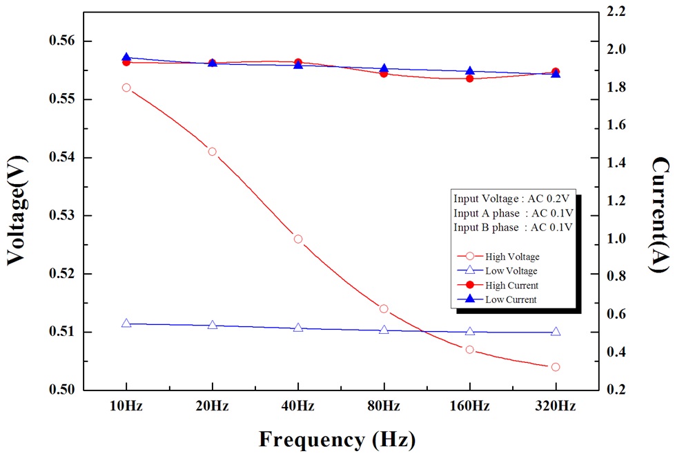
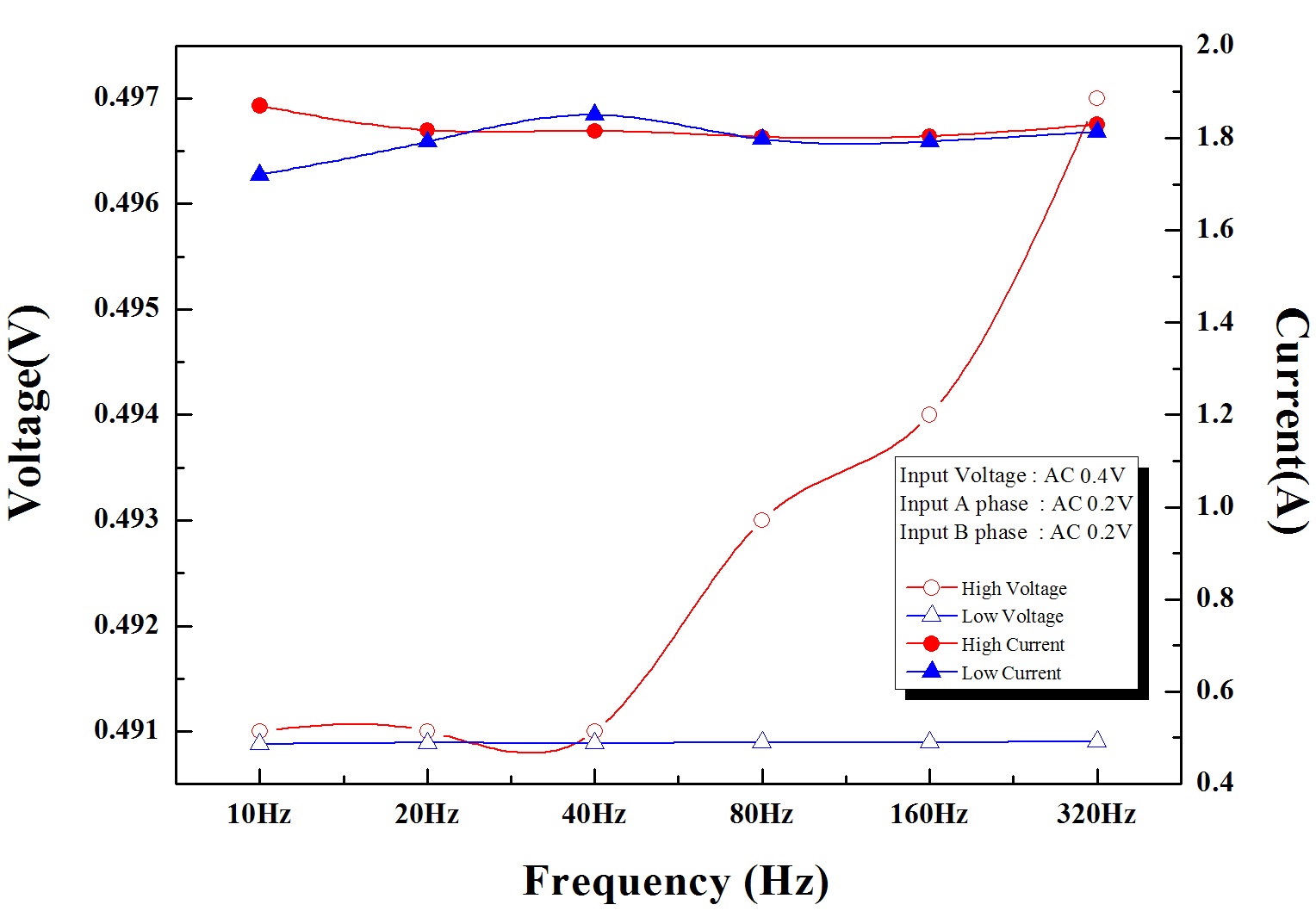
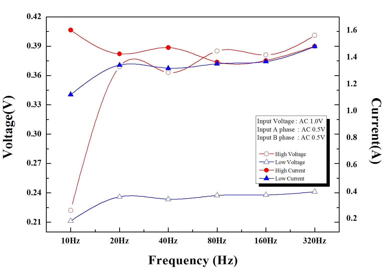
Figure 3~9 shows of the experimental results such as this research. The capacitance of silicon solar cell can be calculated about information of the occurred physical state in the energy band.
Also, this information can possible of analysis as reliable form from occurring carrier density with sunlight absorption [3]. In addition, If the changes in the area of the solar cell, capacitance formation of depletion region and it directly related bring something on changes of charge density [4].
In the depletion region of the silicon solar cell, charge density of the semi-stabilized is formed to potential difference of small range and it open voltage and short current output gave a directly
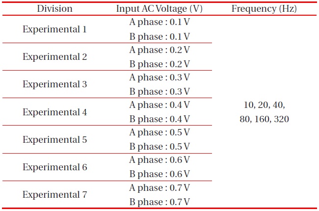
Alternating current(AC) voltage input parameter for controlling the capacitance of the silicon solar cell.
effect. The power conversion was changed by alternating current(AC) voltage bias of 0.2~1.4 V and 6 frequency band characteristics, changed capacitance of depletion region could be observed by the indirect method of direct current(DC) voltagecurrent.
Such as the foregoing, discussion on the results of this paper will be discussion about changing direct current(DC) voltagecurrent of electric field by changes capacitance in depletion region. The depletion region is defines a stationary state of donor and acceptor ion in the microscopic space-charge region.
Such as results of this experiment, when analyzing of the power conversion output characteristics of between the 6 frequency band of 10~320 Hz, changed frequency per second shown to be provide of direct cause in the charge density changes. In the experiment results of each in Table 1, when input frequency of 10 Hz, maximum current and minimum current show fluid, increasing of frequency, at 320 Hz, current measurement range was reduced. As confirmed from this phenomenon, capacitance of the depletion region, because of changed frequency effect and it effect suggest of a directly cause in the charge movement.
In addition, The charge can be easily moved along the alternating current(AC) voltage signal in the forward bias of low frequencies and it does not react easily by the high-frequency condition [5].
Additional studies of the capacitance which in the changes the bias state, the capacitance density by the positive and negative voltage state showed conflicting results. From the results of this study, as positive bias voltage increases, the capacitance density showed the increasing influence [6].
On the other hand, in the measurement of open voltage of the
silicon solar cell could be observed of rapid changes. Essentially, in the characteristics of the diode, when applied in the reverse direction of alternating current(AC) voltage, which have rectification character and it show because of the gave to directly effect of charge distribution in the close-set charge of depletion region. In the analysis of equilibrium state, reverse bias stage, forward bias state of the Silicon p-n junction diode, the most emphasis analysis is changes of potential barrier. An applied of forward and reverse bias gave a direct effect in the width change of depletion
region. An applied voltage in the externally has been known to the transformative of electrostatic potential barrier. Because physical phenomenon, transformative to the charge density in the transition region, several components of the current was demonstrated to changes [7].
Thus, Hammond, P presented can be defined by equation -6 which is the energy of the electric field.

The occurrence source of this energy between the conductors of capacitor is performed by outside influences.(optically absorption and power apply) And In the p-n junction of depletion region, because of the changed electric field is not relationship continuous charge release by outside influences.
In addition, When the electric field energy is permission moving equilibrium position, it is freedom is preserved. This energy is completed in the corroborated electric field [8]. The changed electric field by ionization carrier in the energy band, gave direct effect on the separation of generated electron-hole pairs due to sunlight absorption and it is directly related to the carrier diffusion and physical value of short current. Because of the characteristics of applied alternating current(AC) voltage, changed
potential barrier shows of value of measured open voltage in the 7 graphs of this paper. When observing the open voltage output of a graph, minimum open voltage results showed a linear form. On the other hand, maximum open voltage showed very irregular and non-linear voltage characteristics results. In the depletion region, Indigenous voltage (built-in voltage) can be applied as follows. First, in the acceptor area, indigenous voltage can be defined as equation -7.
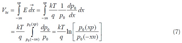
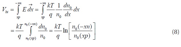
In succession, indigenous voltage of the donor area can be defined as equation (-8)
When external voltage is applied such as this experiment, indigenous voltage change can be deployed as equation-9.
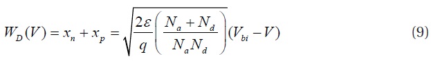
In this equation, because effect of ionization carrier is generated to inside electric field and the internal electric field provide of carrier separated of electron-hole pair. The V applying of external voltage show directly effect on the inside potential difference decreases.
Because of the applied effect of alternating current(AC) voltage in the depletion region of the silicon p-n junction, by changed frequency effect of every second unit could be an indirect confirmation to changing a potential difference.
Also, current output such as movement of carrier diffusion could be confirmed by indirectly method of physical interruption factor by locally. The potential difference between two junctions in the depletion region, when the charge density of acceptor and donor ion is always constant which voltage output is constant output. However, the open voltage of solar cell in this experiment showed always irregular measured result. The optically absorption of electromagnetic radiation to a silicon crystal lattice caused the photoelectric effect of the ground state carrier. The bias input in both ends of the silicon p-n junction semiconductor is basically generate of carrier drift current and diffusion carrier which is obtained for the energy of the electric field and carrier movement can think to the acceleration. The character of the alternating current(AC) voltage is change to phase of every second cycle. therefor, In the depletion region of solar cell is temporally generated of the forward bias and reverse bias. Accordingly, the capacitance of the depletion region is affected. When applied alternating current(AC) voltage to the solar cell is saturation state, carrier movement not formed to any more. When saturation state of the applied alternating current(AC) voltage of solar cell is not any more formed to carrier movement. The saturation state of alternating current(AC) voltage is defined higher applied than generated voltage difference by silicon p-n junction. When the experiments to higher voltage than maximum voltage 1.4 V was temporarily inoperative to square wave generation equipment.
The excessive alternating current(AC) voltage is applied in the silicon solar cell, capacitance effect of depletion region is defined to the effect to completely lost. The disable operation state of square wave generation equipment is defined to inability of insulators function as capacitance charge of large number concentrated of silicon p-n junction.
Typically, in the depletion region of silicon p-n junction is defined to the breakdown as physical effects. Because of the influence to alternating current(AC) voltage with a square wave pulse is decreasing of excess carrier separate. And in the movement of carrier diffusion did not get enough acceleration force which power conversion process can be analysis as affected.
So far, as described qualitatively in the results for this experiment, understanding for internal structure of capacitor using passive element in the R.L.C circuit was analyzed for power conversion with changed capacitance.
Using a square wave of 10~320 Hz frequency and an alternating current(AC) voltage source of 0.2~1.4 V, in the depletion region of the silicon p-n junction solar cell was analyzed to the character of power conversion of silicon solar cell. In the master course thesis theme of the author’s with solar cell research of compound semiconductor for high efficiency power conversion [9] was performed to the experiment by extending to uncompleted portion. Mainly, in the depletion region of the hetero-junction, charge density and changed electric field were analyzed to quantitative calculation and capacitance term of diode depletion region has not exact mention.
Therefore, in this paper, along with the changes of charge density which is directly related to the power conversion efficiency, and directly controlled by the capacitance of the depletion region, power conversion of silicon solar cell could be analyzed as such this results.