Recently, carbon material has attracted great interest as a semiconductor material due to its attractive properties arising from the adjustable ratio of sp2 and sp3 carbon bonding ratio. Amorphous carbon (a-C), one of the carbon branch is said to have the mixture of sp2, sp3 and even sp1 carbon sites, which allow the properties of the a-C to be tuned as desired [1]. The a-C material has a semiconducting nature which enable the material to accept dopants [2], and wide band gap from 0.0 eV to 5.5 eV [3]. The deposition parameter of a-C is also compatible with glass substrate which is cheap since the production can be as low as 350℃.
Researchers have developed many useful techniques to prepare the a-C, such as physical vapour deposition techniques, direct current (DC) and radio frequency (RF) magnetron sputtering, electron cyclotron resonance, ion beam or ion beam assisted deposition and reactive pulsed laser deposition (PLD). As an alternative, the low cost chemical vapor deposition (CVD) technique has also been employed in the fabrication of a-C. However, some problems limit the use of the CVD method, such as the lack of proper volatile precursor and the difficulty in controlling the stoichiometry of the deposition [4]. These problems were countered, by modifying the conventional CVD process into aerosol-assisted CVD (AACVD), where this method uses the aerosol droplets to transport the precursor, with the aid of the carrier gas.
Nano-structured material is attracting great interest among researchers, and the modification of the conventional CVD into the AACVD is one of the efforts to produce nano-structured based material. Based on the review, the AACVD technique has the ability to produce nano-structured materials, as reported by Salaun et al. [5] and Qureshi et al. [6]. The a-C material, having the amorphous nature is very hard to obtain in a nano-structured form, however the application of AACVD is expected to cope with the problems. In the case of using the a-C in a solar cell application, nano-structured a-C has many advantages, such as the optical absorption path being much larger [7], the absorber layer baing thin, thus the light generated electrons and holes will only have to travel over a much shorter path and thus the recombination losses are greatly reduced [8] and the energy band can be tailored by varying the size of nanoparticles, thus more designs of the absorber layers in the solar cell can be done [7].
In this experiment, we have investigated the application of AACVD to produce the nano-strustured a-C, as well as using the same technique to dope the a-C into an n-type a-C. Nitrogen gas, N2 was used as the dopant, and a-C:N was produced. The a- C:N has an interesting properties, from large photosensitivity up to 6.2 eV, photoluminescence up to 4.5 eV, a high resistivity and low dielectric constant [9]. Nitrogen-containing carbon was proposed from different type of precursors, for example acetonitrile, pyrole or polyacrylonitrile [10-12]. However, we managed to deposit the nano-structured a-C using the natural precursor camphor oil, and the change in structure of a-C and a-C:N was highlighted by the Park System XE-100 atomic force microscopy (AFM) and field emission scanning electron microscopy (FESEM) characterization. On the other hand, the electrical and optical properties of both conditions were investigated by using the Bukoh Keiki CEP2000 solar simulator system at room temperature and Perkin Elmer LAMBDA 750 UV-vis-NIR spectroscopy.
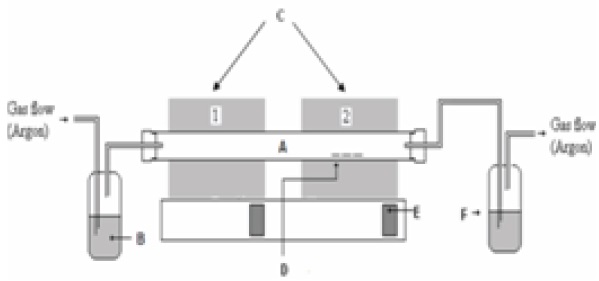
The a-C and a-C:N were prepared using Aerosol-assisted CVD (AACVD) with the precursor of camphor oil (C10H16O). The glass substrates were cleaned by acetone (C3H6O) and methanol (CH3OH) for 10 min respectively using an ultrasonic cleaner (Power Sonic 405) to eliminate contaminations. Lastly the substrate was blown with nitrogen gas (N2). The AACVD combines the application of the conventional CVD system and the spray pyrolysis method, with the aid of the carrier gas. For the pure a-C, argon gas which is an inert gas was employed as the carrier gas, whereas for the N doped a-C:N the nitrogen gas was selected as the dopant gas, which also acted as the carrier gas. The main purpose of the carrier gas is to carry the camphor oil in gaseous form from the aerosol part towards the heated substrate in the CVD. The precursor was first heated up to its vaporization temperature (180℃) to transform the liquid form into the gaseous form. The deposition temperature at furnace two was varied from 400℃ to 600℃, with 5 samples each for the a-C and a-C:N. The thickness for the samples was measured by the surface profiler DEKTAK VEECO 150 and the thickness was from 30 nm to 70 nm. During the deposition process, furnace one at the CVD system was set at 200℃ to help the atomization of the camphor oil. The deposition took place for 30 minutes. A schematic diagram of the AACVD system is shown in Fig. 1.
The electrical and optical properties of deposited a-C and a-C: N thin films were characterized by Bukoh Keiki CEP2000 solar simulator system at room temperature and Perkin Elmer LAMBDA 750 UV-vis-NIR spectroscopy, whereas for the structural properties, the Park System XE-100 atomic force microscopy (AFM) and field emission scanning electron microscopy (FESEM)
were used. In this experiment, the nano-structured properties were confirmed from the structural measurement, and the successful doping was clarified as shown from the differences in electrical and optical properties of the a-C and the a-C:N.
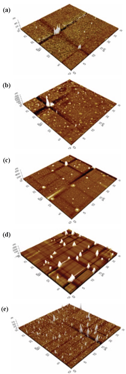
The measurement for structural properties was carried out by Atomic Force Microscopy (AFM). Figures 2 and 3 shows the three-dimensional (3D) structure of the a-C and a-C:N at 5 different deposition temperatures, (a) 400℃, (b) 450℃, (c) 500℃, (d) 550℃, and (e) 600℃ (thickness 30 nm to 60 nm). Based on the images, the topography between undoped a-C and nitrogen doped a-C:N shows significant difference which will be explained later.
For pure a-C, there are irregular structures of the a-C, with only the growth of an “island” structure at 400℃, however as the temperature increase the structure becomes more even. There are some aggregation spots of in samples 400℃, 450℃ and 500℃, which might be due to improper dispersion of the carbon atoms. At 550℃ and 600℃, the growth of a-C started to develop smoothly as compared to the other samples. The AFM average roughness was estimated over a 30 μm × 30 μm area and the roughness was not really dependent on the deposition temperature. From 400℃ the average roughness was 0.361 nm, and then the value rises to 1.080 nm, 2.147 nm, 8.219 nm and 0.391 nm. However, for sample 400℃ and 600℃, we can clarify that the small value was caused by a different aspect, where at 400℃ we can say that the small roughness value was because of the improper growth of the carbon atom, and at 600℃ actually the sample is smooth and thus the roughness is small. For sample 550℃, the surface migration of the a-C particle is said to be enhanced, thus the particle combines to create large particles, as compared to the lower deposition temperature [13]. On the other hand, as the temperature gets higher at 600℃, it is clearly shown that the sample becomes smoother, and that could be related to the increase of energetic carbon ion bombardment at the surface of the thin film [14].
Nitrogen doped a-C:N as in Fig. 3, shows uniform AFM images at sample 500℃, 550℃ and 600℃, but aggregation was seen at sample 400℃ and 450℃. There was some carbon patches at the surface of both samples, and at 450℃, only a carbon ‘tower’ can be seen at the centre of the area, whereas at the surroundings, no sign of carbon growth was evident, which illuminates the inappropriate growth of carbon in the sample. The average roughness indicated was relatively small, ~0.00 nm to 1.463 nm, and was not dependent on the deposition temperature. Figures 3(a) and (b) displays an uneven dispersion of carbon particle; however as the temperature got higher, the structural properties of the a-C:N
[Table 1.] Roughness value of pure a-C and nitrogen doped a-C:N.
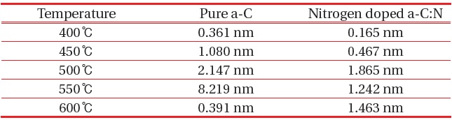
Roughness value of pure a-C and nitrogen doped a-C:N.
improves thus clarify that lower temperature was not suitable for the a-C:N growth. Other than that, at the same deposition temperature, a-C:N has better structure as compared to the pure a-C. Small roughness indicates the lower grain boundaries, which can be related to the tendency of the particle to become more crystallite [15]. The roughness value obtained was similar to the one reported by Miyajima et al. [16]. Table 1 provides the average roughness value for numerical comparison.
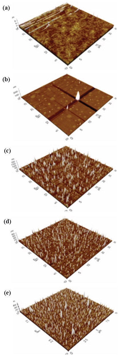
Figure 4 shows the FESEM images results of both a-C and a- C:N at 100 K magnification and 10 kV. Both condition have a
small average grain size, approximately ~50 nm to claim that the a-C thin film structure is nanostructured (less than 100 nm). The pure a-C sample has an agglomerated particle, whereas the a-C:N has a bigger and flawless particle (but still less than 100 nm) with cylindrical shapes. The clear and flawless particle results from the high kinetic energy gained by the particles, which makes it easier for the particles to migrate on to the surface and easier for them to grow [17]. For the a-C solar cell application, the nanostructured material has some promising advantages, such as that the optical absorption path is much larger [7], and the absorber layer is thin, thus the light generated electrons and holes will only have to travel over much shorter path and thus the recombination losses are greatly reduced [18], and the energy band can be tailored by varying the size of nanoparticles, thus more designs of the absorber layers in the solar cell can be done [7]. Other than that, the successful doping condition for the nitrogen doping is confirmed through the FESEM spectrum results, with the presence of the nitrogen (N) element in the a-C:N sample.
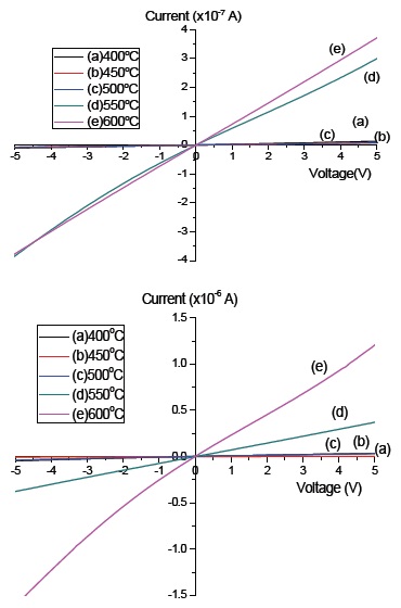
The electrical properties were measured by the solar simulator system, and for both the pure a-C and the a-C:N, an ohmic graph were obtained, as in Fig. 5. The supply voltage was set from -5 to 5 V. From graphs (a) and (b), the pure a-C has slightly lower current value, as compared to the a-C:N. Gold (Au) was used as the counter electrode, with a thickness of 60 nm. The current obtained for pure a-C was ×10-7 A, whereas for the a-C:N when nitrogen was used as the dopant/carrier gas the current value was 10-6 A. Both a-C and a-C:N were deposited on glass substrate at 5 different deposition temperatures (400℃, 450℃, 500℃, 550℃, 600℃). The highest slope of the ohmic graph was obtained at sample 600℃, and the slope reduces as the deposition temperature increases. The higher slope indicates a lower resistance value. The values of resistivity (ρ) and conductivity (σ) were calculated from the value of resistance using equation (1) and (2) respectively, where R is the resistance obtained from the I-V curve, w is the width of the electrode, t is the thickness of the a-C thin film and L is the length of the electrodes.


For the pure undoped a-C, the conductivity (σ) was calculated and the highest conductivity was 9.4×10⁻² Scm-1 at 600℃, followed by 7.1×10⁻³ Scm-1 at 550℃, 1.9×10⁻⁴ Scm-1 at 500℃, 2.2×10⁻⁴ Scm-1 at 450℃ and 1.8 ×10⁻⁴ Scm-1 at 400℃. On the other hand, the conductivity shows the same increment as the temperature increase in a-C:N, 3.9×10⁻² Scm-1 at 600℃, followed by 9.1×10⁻³ Scm-1 at 550℃, 2.2×10⁻³ Scm-1 at 500℃, 1.9×10⁻³ Scm-1 at 450℃ and 4.7×10⁻⁴ Scm-1 at 400℃. The electrical properties can be produced theoretically from the density changes of the crystal defects, such as the vacancy, grain boundary and film surface, which in turns, can also be directly related to the carrier concentration and mobility of the electron at different thickness of thin films [19].
The samples deposited under nitrogen gas as the dopant/carrier gas exhibit larger conductivity due to the fact that nitrogen gas as the dopant gas for the a-C can tune the conductivity of pure a-C from p-type into n-type material. The successful doping is said to decrease the defects since the spin density gap decreases with the nitrogen addition [20]. Other than that, the nitrogen addition is also confirmed to decrease the compressive stress of the films and leads to the increase of conductivity [21]. Further, the slow increase of the electrical conductivity is due to the removal of the structural defects and improvement of structural order as discussed above. Thus this has become the reason for the higher conductivity of nitrogen doped a-C:N.
Increasing deposition temperature leads to higher thickness value (confirmed by the measurement by surface profiler). The carrier concentration and carrier mobility was reported as the important reason in conductivity variation [22]. As the thickness increase, the carrier concentration and carrier mobility will increase [19]. Other than that, a-C conductivity is also attributed to the presence of π* (sp2 graphitic bonding) and σ* (sp2 and sp3 diamond bonding). As temperature increases the intensity of the π* region increase, specifying the promotion of sp2 bonding due to the increase in graphitic order [23]. The a-C and a-C:N material has a mixture of sp2 (graphitic) carbon bonding and the ratio can be modified depending on the deposition condition for such the deposition temperature [24]. As temperature increase, the conductivity was said to increase. The higher conductivity of a-C and a-C:N films at higher temperature (600℃) was because of the complete separation from the precursor atom to produce the carbon atom and also the formation of more sp2 carbon bonding sites. The formation of more sp2 carbon bonding sites resulted in the increase of the localized hopping states [25]. At lower temperature the a-C is attributed to have a higher sp3 carbon bonding ratio, thus explaining the lower conductivity at lower temperature.
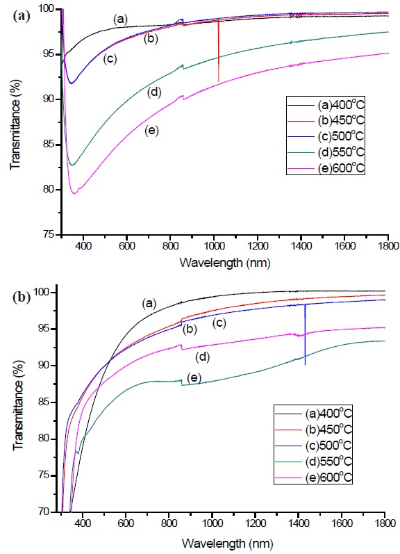
The optical properties of the a-C and a-C:N thin films were investigated by UV-vis-NIR spectroscope using thin films deposited on glass substrates, in the wavelength range of 300-1,800 nm. The Tauc optical band gap was derived from the optical characterizations. It is observed that the optical transmittance had a high value (>80%) at the visible range 390 to 790 nm (1.56 to 3.18 eV), which contain the largest amount of energy based on the solar spectrum. Figures. 6 (a) and (b) show the transmittance spectra of a-C and a-C:N. For the pure a-C samples, an obvious difference appeared between the samples, with the highest transmittance being at sample 400℃, and those at sample 450℃ and 500℃ intercept each other. The lowest transmittance appears at 600℃, with approximately 80%-85% in the visible range. On the other hand, the a-C:N has high transmittance for all the samples, but the trends were not as obvious as for the a-C thin films. The highest transmittance was noted at sample 400℃, and the lowest was at 600℃.
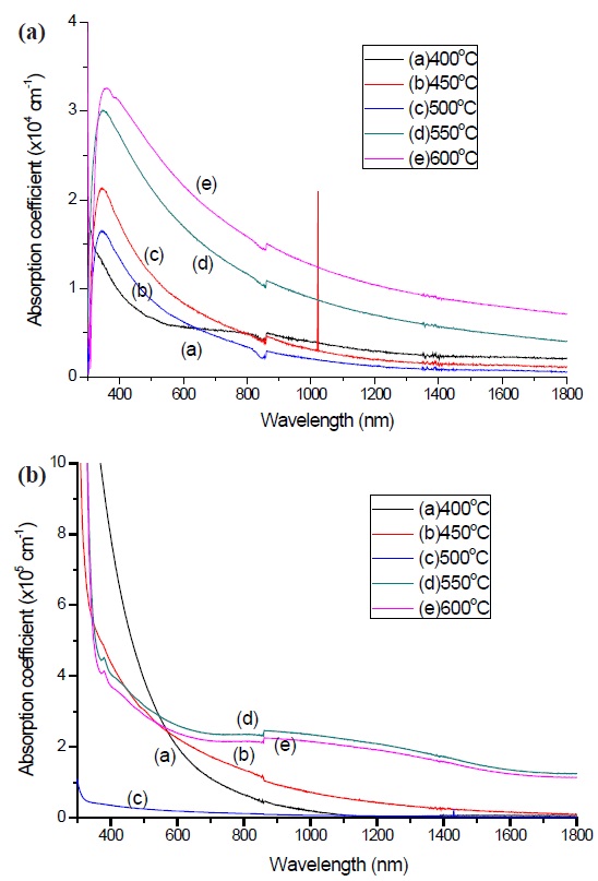
The absorption coefficient, α of a-C thin films could be calculated by Lambert’s Law using

Where, t is the thickness and T is the transmittance of the film. Pure a-C exhibits an α of 104 cm-1, and the nitrogen doped a- C:N has shown an increment in the value, α of 105 cm-1. The α is explained from the ability of the material to absorb the photon energy from light and thus the higher the α, the better the performance of the films. The high α value is ascribed to the presence of more graphitic component (sp2 carbon bonding) in the carbon films [26]. Based on Figs. 7 (a) and (b) the α value at the visible range is the highest, since this wavelength contains the highest amount of energy. A similar α was determined by other researchers [26,27]. From the calculated absorption coefficient, the optical band gap was determined using the Tauc relation [28].

which corresponds to the indirect optical band gap in an amorphous semiconducting material [29]. Figures. 8(a) and (b) represents the Tauc plot for determination of the optical band gap of the pure a-C and nitrogen doped a-C:N. It was noted that both conditions have decreasing values as temperature increases, and the optical band gap for both cases are approximately 1.4 eV at 400℃, and as the temperature increase, the value decrease to approximately 0.3 eV at 600℃. The largest optical band gap is correlated with the amount of sp3 carbon bonding inside the a-C and supports the electrical conductivity discussed above. The modification of the optical band gap might be due to the structural changes, as discussed above. According to Tay et al. [30] and
[Fig. 8.] Tauc plot of (a) pure a-C and (b) nitrogen dope a-C:N at different deposition temperature.
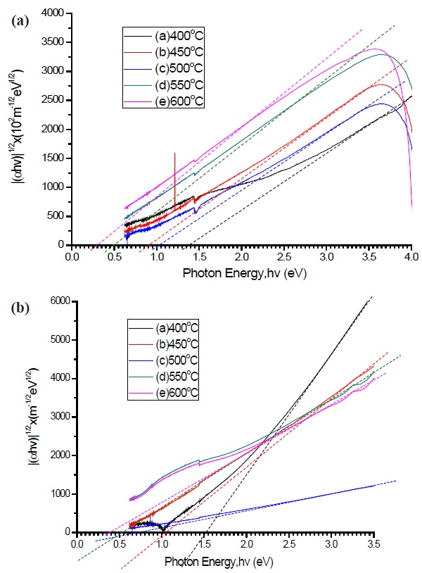
Cheah et al. [31], the modification of the optical band gap edge is attributed to the removal or creation of band tail states, and the material is assumed to have less band tail states when the edge has an increase in slope.
Nanostructured a-C and a-C:N thin films with small particle size, ~50 nm were obtained by Aerosol-assisted CVD method from the natural precursor camphor oil. From the FESEM images, flawless and clear images were obtained for the a-C and a-C:N, due to the high kinetic energy gained by the particles and thus making it easier for the particles to migrate on to the surface and easier to grow. The AFM images have variation in the roughness value, depending on the deposition temperature of the pure a-C and the nitrogen doped a-C:N. At high temperature, the AFM clarifies an even smoother image, due to the increase of the energetic carbon ion bombardment at the surface of the thin film. An ohmic contact was acquired from the current-voltage solar simulator characterization, using gold (Au) as the counter electrode. Higher conductivity at a-C:N is due to the decrease in defects since the spin density gap decreases with the nitrogen addition. Also, the nitrogen addition decreases the compressive stress of the films and leads to higher conductivity. Pure a-C exhibita an absorption coefficient, α of 104 cm-1, whereas for a-C:N, α is of 105 cm-1. The high α value of a-C:N is due to the presence of more graphitic component (sp2 carbon bonding) in the carbon films.