With the recent increase in industrial and economical interest and investment in new and renewable energy, a great deal of development is occurring in the research and industrialization of photovoltaic devices, which is a representative clean form of energy production. The competition to develop a more efficient and cost-effective solar cell remains intensely. Research is especially lively in the area of analysis of the behavior of the photovoltaic effect on the nano scales for the development of tailored photoelectric materials and the development of competitive solar cell manufacturing processes through optimization.
The methods of analyzing the photoelectric effect, the basic principle behind the operation of the solar cell, and its mechanism, have been developed and improved together with the progress of photovoltaic power generation [1-4]. Among these methods, photoconductive atomic force microscopy (PC-AFM) is a type of SPM analysis method developed for property analysis of photovoltaic elements. With a composition based on the principles and devices of conductive AFM, it employs an additional attached light source to shine light onto the photovoltaic element. Normally, the light source is located beneath the specimen, and light is shone onto the specimen through a transparent conductive oxide. Through this device, the conversion efficiency of solar cells can be analyzed at the nano level, and visual analysis of phase separation, charge generation, charge transport, and charge collection can be performed. Also, using a monochrometer with wavelength modulation, this method is especially useful in studying the relationship between morphology, material composition, and light wavelength that impacts the photocurrent generation of the specimen [5-8].
In this study, PC-AFM, a recent noteworthy method for nanoscale characterization of photovoltaic elements, was used for direct measurements of the photoelectric characteristics in local instead of large areas. The effects of changes in the intensity and wavelength of light shining on the element on photoelectric characteristics were observed. Results gained through PC-AFM were compared with the electric/optical characteristics data gained through a solar simulator.
To investigate the effect of light intensity and wavelength of the solar cell device by using the PC-AFM, we prepared p-n junction-structured poly-Si wafer-based solar cell devices. A 200 nm-thick poly-Si wafer was heated in a diffusion furnace at temperatures up to 850℃ with POCl3 to form a p-n junction on the surface of the wafer using the diffusion process. The thickness of the diffused n-type region was about 300 nm, and its sheet resistance was about 60 Ω/□.
The dimensions of the fabricated solar cell were 2 ㎝ × 2 ㎝, the thickness of the antireflection layer (SiNx) that was deposited by plasma enhanced chemical vapor deposition process was 76 nm, and its refractive index was 1.97. After deposition of the SiNx layer, the bottom and top electrodes were connected by screen printing with the silver paste, and the thicknesses of the bottom electrodes and the top electrodes were 60 ㎛ and 20 ㎛, respectively. For the formation of the ohmic contact for the electrodes, devices were annealed in 680℃ with rapid thermal processing [9]. The electrical properties of prepared solar cells were measured using the K201 solar cell simulator system (McScience Inc., Korea), and the results are summarized in Table 1. The average open circuit voltage (Voc) was 0.49 V, and the average short circuit current (Isc) was 41.3 mA. Also, the average values of fill factor and efficiency of the six devices were 0.7% and about 13.6%, respectively. In addition, the external quantum efficiency (EQE) (which is the ratio of the number of charge carriers collected by the solar cell to the number of photons of a given energy shining on the solar cell from outside), was analyzed, and the results are shown in Fig. 5.
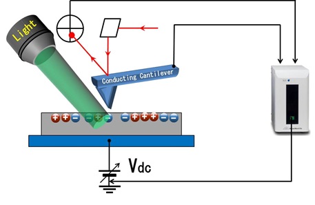
The following experiment was performed using the Seiko Instrument E-sweep SPM model, interfaced with an external light source and solar simulator to observe the effects of light intensity and wavelength on photoelectric effect characteristics (Fig. 1). First, a solar simulator was used to vary the intensity of light shining on the solar cell from 0 ㎽/㎠ to 130 ㎽/㎠ in 10 ㎽/ ㎠ increments and measure the resulting I-V characteristic curve. From this result, the Voc values corresponding to each level of light intensity were extracted. For PC-AFM analysis, light intensity was increased from 0 ㎽/㎠ to 16 ㎽/㎠, and the AFM system was used to measure the I-V characteristic curve. Here, the cantilever tip used as the electrode was a diamond tip doped with boron. The I-V measurements taken with PC-AFM were used to extract the voltage (VPC-AFM), of which the current was 0 A. This was presented against light intensity in a graph, and these results were compared with measurements from the solar simulator.
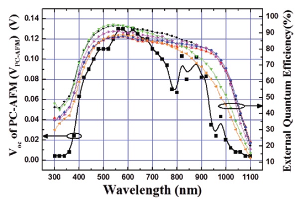
Also, to analyze the behavior of photoelectric characteristics in response to the wavelength of light shining on the solar cell device, the following measurements were made. Using the monochrometer attached to the PC-AFM, light wavelength was varied from 300 ㎚ to 1,100 ㎚ in 20㎚ intervals, and the I-V characteristic curve was measured. Similar to the measurements described above, a diamond tip was used. The VPC-AFM value at each wavelength
was extracted from the I-V measurements and presented in a graph (Fig. 5). These measurements were compared with EQE characteristics.
The p-n junction-structured poly-Si-wafer-based solar cell devices were fabricated using a POCl3 diffusion process. The electrical properties of the prepared solar cell devices were measured, and the results are shown in Table 1. The Voc is 0.59 V and the Isc is 48.5 mA. Also, the values of the fill factors and efficiencies of the devices are 0.7% and approximately 13.6%, respectively.
In addition, when light with a wavelength of 540 nm was used to irradiate the devices, the maximum values of the EQE (95%) were attained. We verified that all of the devices had similar electrical and optical properties [9].
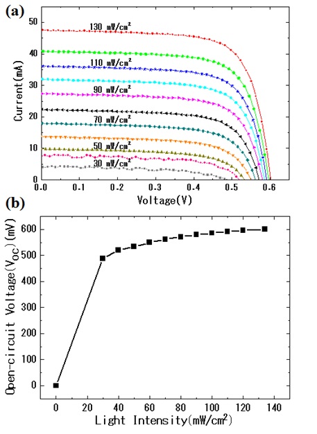
Figure 2 presents the I-V characteristic curves of poly-Si solar cells measured at various irradiation intensities. In the case where the voltage applied was zero, the Isc value linearly increased according to the light intensity. Voc, the value of the voltage applied with the corresponding current being zero, remained between 0.5 and 0.6 V, with its change indicated in Fig. 2(b).
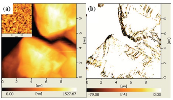
The poly-Si-based solar cells were scanned using PC-AFM, and the topology and the current images were simultaneously obtained with 0 V DC bias under light irradiation as shown in Fig. 3. In the current-mapping image, the dark areas or spots indicate the flow of a more vertical current through the cell surface when compared with the bright area.
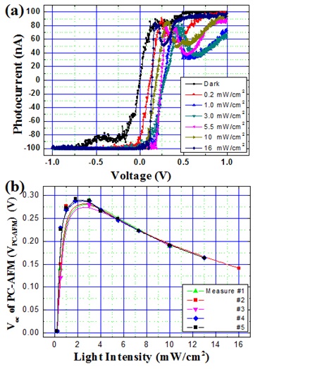
For analysis of the photoelectric effect in response to light intensity, light at 0.2, 0.5, 1, 1.8, 3, 4, 5.5, 7.3, 10, 13, and 16 ㎽/ ㎠ intensities was shone on the solar cell. Using a diamond tip as the electrode, the I-V characteristic curves were measured. From these results, the voltage (VPC-AFM) at which the current was 0 A was extracted and is presented against light intensity in a graph (Fig. 4). Comparison of solar simulator analysis and PCAFM analysis results confirmed the following. First, in the solar simulator measurements, the Voc value increased dramatically when light intensity increased from 0 ㎽/㎠to 30 ㎽/㎠. After this point, Voc increased at a low slope in response to increased light intensity, and tended to saturate. Voc at 30 ㎽/㎠ was 0.47 V, and the maximum Voc value was 0.58 V.
On the other hand, in the PC-AFM measurements, VPC-AFM increased sharply up to 1.8 ㎽/㎠, peaking and slowly falling as light intensity increased. Here, VPC-AFM at 1.8 ㎽/㎠ was 0.29 V, which corresponds to 59% of the average Voc value as measured with the solar simulator. It is believed that the VPC-AFM value measured
[Table 1.] Electrical properties of poly-Si solar cell devices.
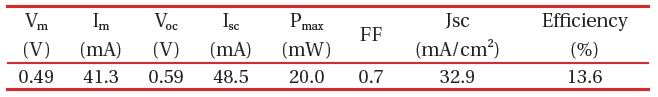
Electrical properties of poly-Si solar cell devices.
with PC-AFM was low because the contact resistance in the areas of contact between the tip and surface of the specimen was larger than the ohmic contact resistance of the electrode used for the solar simulator measurements. It is also believed that the tendency for the VPC-AFM values extracted from PC-AFM to decrease with increasing light intensity is because of the formation of a SiO2 oxidation layer formed on the Si surface of the solar cell when the current flows from this surface to the diamond tip [10-13]. Repeated I-V characteristic curve measurements were taken with the cantilever tip contacting the identical position on the specimen’s surface. With the accumulation of the oxidation layer, contact resistance and voltage drop both increased. It is speculated that this resulted in the slow, downward trend of VPC-AFM.
The following measurements were then made to analyze photoelectric characteristics behavior in response to light intensity as measured with EQE and PC-AFM. After measuring the I-V characteristic curve while increasing the wavelength of light shining on the solar cell from 300 nm to 1,100 nm in 20 nm intervals, VPC-AFM was extracted similarly to the previous analyses. Figure 5 presents the EQE and PC-AFM analysis results for the same wavelength range. Both measurements were made for wavelengths in the range of 300 nm to 1,100 nm; also, between 300 nm and 700nm, it was seen that the EQE value and VPC-AFM value exhibited almost identical trends. However, VPC-AFM decreased
by a larger rate than the EQE results beyond 700 nm. Unlike the EQE results, VPC-AFM showed oscillating behavior between 800 nm and 950 nm.
The cause for this difference in behavior between the two measurements has not yet been identified. Additional research is required on whether this effect on repeat I-V characteristic curve measurements is the result of variations in electric and optical characteristics between the local area where the tip contacts the specimen, mechanical vibrations, or unstable light factors. In order to overcome this limitation, a method of measurement wherein the wavelength of light shining on the specimen sweeps within a certain range allowing for direct extraction of VPC-AFM values would be required. However, despite these measurements, it has been confirmed through these results that the PC-AFM measurements were macro in scale, similar to the EQE analysis results. The potential of PC-AFM as a useful method of analysis in the measurement and analysis of photovoltaic characteristics
in response to wavelength variations of light at the nano scale was confirmed.
In this study, the POCl3 diffusion doping process was used to produce a p-n junction solar cell device based on a Poly-Si wafer. In terms of the electric characteristics of this solar cell, Voc was 0.59 and Isc was 48.5 mA. The fill factor and conversion efficiency were 0.7% and 13.6%, respectively. We used the solar simulator and PC-AFM methods to analyze the photovoltaic characteristics of this device. By comparing changes in Voc and VPC-AFM from the PC-AFM method in response to increasing light intensity, we confirmed that in PC-AFM measurement, the contact resistance between the tip and surface of the specimen, and the generation of an oxidation layer from the current, impacted on the characteristic analysis.
In addition, while the light wavelength was increased from 300 nm to 1,100 nm, the two measurements showed similar trends at the macro scale, but returned different results in several sections, indicating the need for detailed analysis and improvement in the future. Through such studies, it was confirmed that the PC-AFM method of analysis maintained a certain correlation with existing solar simulator research, and its advantage is that it is the only method of direct observation and comparison of the photovoltaic effect in specific local areas at the nano scale. This implies that PC-AFM could be indispensable in the analysis of photovoltaic mechanisms for new photovoltaic material development and process optimization required for future progress in solar cell technology.