The increasing demand for fossil fuels and the environmental impact of their use are continuing to exert pressure on an already-stretched world energy infrastructure. Significant progress has been made in the development of renewable-energy technologies, such as solar cells, fuel cells, and biofuels. Dyesensitized solar cells (DSSCs), invented by Graetzel and O’Regan in 1991, have paved the way to cell efficiency, reaching as high as 11% and allowing us to foresee the possibility of obtaining cost efficient cells [1]. Cost effectiveness is an important parameter for producing DSSCs, compared to widely-used conventional silicon solar cells. DSSCs consist of wide bandgap nanoporous metal oxide films, such as TiO2 deposited on a conducting oxide layer, as electron transport layers. DSSCs have attracted considerable attention owing to their simple fabrication process, low production cost, and applicability to flexible substrates [2].
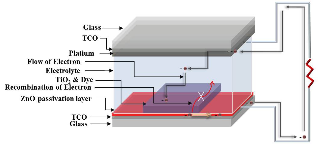
Many studies have reported the electrode modification of DSSCs. Electrode modification is performed in order to decrease electron loss at the interface between the TCO and the electrolyte [3]. A dense film was found to lead to faster electron transport and slower recombination; electron transport was slower in more porous films. Therefore, dense film between the TiO2 electrode and transparent conducting oxide can be useful [4]. In this study, ZnO thin films are used as a compact layer in DSSCs [5]. Using a Zinc Oxide (ZnO) passivating layer prevented the loss of electrons and improved efficiency of DSSCs. ZnO nanoparticles have a hexagonal structure, which promotes optical refraction [6]. The ZnO passivating layer was prepared on FTO glass, by RF-magnetron sputtering. ZnO thin films, produced by the RFsputtering technique, have advantages such as homogeneity, high purity, and the nanostructured features of thin film [7]. The RF-sputtered ZnO film structure operated as an effective electron recombination circuit preventive layer (passivating layer) between the FTO and the electrolyte.
ZnO passivating layer thin films were prepared by RFmagnetron sputtering, using a ZnO target (99.99% purity, LTS Research lab., Inc), 2’’ in diameter and 1/4’’ in thickness. FTO (20 × 20 mm2 9 Ω/sq SnO2:F) glass was used as the substrate, and the substrate surface was cleaned with ethanol and sonification
in isopropyl alcohol. The FTO glass substrates were inserted in an RF-magnetron sputter chamber at a distance of 10 cm from the substrate. The vacuum in the chamber was 5 × 10 6 torr of the base pressure. Deposition was performed at a pressure of 5 mTorr in argon-oxygen atmosphere at an RF power of 80 W, with additional changes at 50 W, 160 W, and 240 W. The ZnO passivating layer was deposited with different working Ar:O2 ratios (1:0, 2:1, 1:1, 1:2, 0:1).
TiO2 powder for the upper layer was prepared by the sol gel method [8]. A 12 μm thick TiO2 nanoparticle upper layer was coated onto the ZnO passivating layer, using a screen-printing method. The TiO2 electrodes were dipped into the 0.5 mM dye complex of N-719 ruthenium(II) (Cis-di (thiocyanato)- N,N’ - bis(2,2’- bipyridyl -4- carboxylic acid -4’- tetrabutylammonium carboxy late) in an ethanol solution, for 24 hours. The counter electrodes were prepared by 5 mM H2PtCl6 ethanol solution, onto FTO glass, and heated at 450℃ for 15 minutes. The dye-adsorbed TiO2 electrodes and Pt-counter electrodes were assembled into a sandwich-type cell and sealed with a hot-melt sealant 60 um thick. The electrolyte was indoctrinated through a hole in the counter electrode, and the hole was sealed using a cover glass. The active area of the solar cells was 0.25 cm2. X-ray diffraction (XRD, Rigaku D/MAX-2200) patterns of mesoporous materials were collected on a Rigaku diffractometer, using Cu K radiation. The morphology and particle size of the ZnO thin film were examined by field-emission scanning electron microscopy (FESEM, EDX, HITACHI S-4700), and surface morphology of the thin films were estimated by atomic force microscopy (AFM). The transmittance of the passivating layer and the absorbance of the DSSC cell were measured using a UV spectrometer (Agilent, UVvis 8453). The photocurrent-voltage measurements were taken using an I-V solar simulator (McScience, Solar simulator).
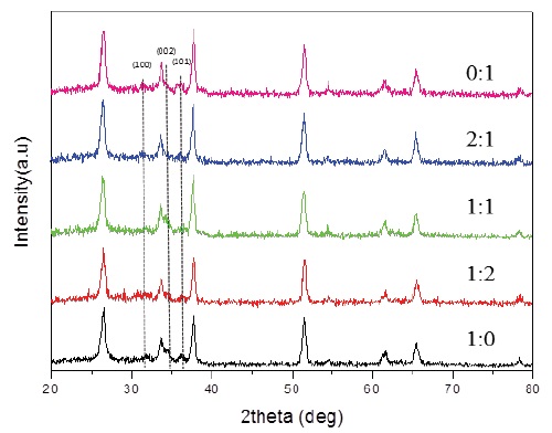
The XRD of the deposited ZnO passivating layer revealed a crystalline structure (Fig. 2). ZnO thin film deposited by RF-magnetron sputtering showed plural ZnO hexagonal wurtzite peaks (002),(101),(100) and FTO, which measured with JCPDS. The peak of the ZnO passivating layer remained almost unchanged under different Ar:O2 ratios and powers.
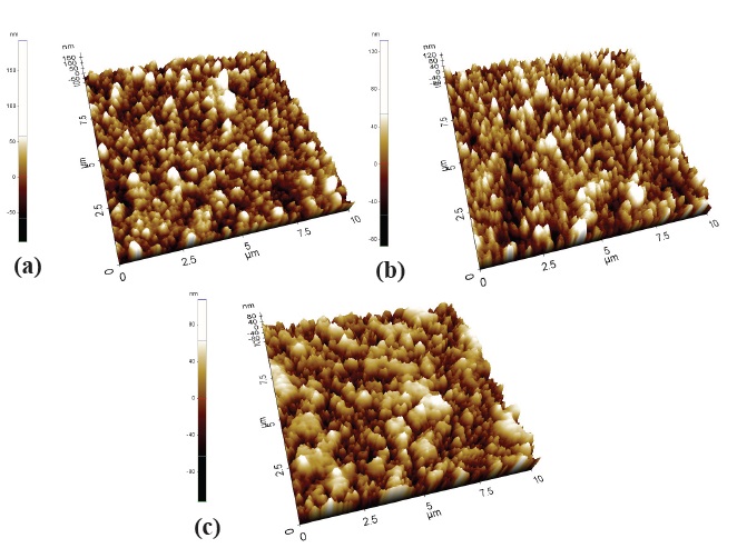
Figure 3 presents the AFM images of ZnO passivating layers. The ZnO thin film deposited using Ar gas only shows a rough surface. The film surface changed to smooth, with an Ar:O2 ratio of 1:1. Then, the surface morphology gradually roughened with increasing O2 flow. The rough surface of the ZnO thin film deposited by using only Ar gas was due to the growth of the pit and the craters which were generated by the resputtering of particles with large sputtering energy. In addition, particle size begins to
grow if the O2 flow ratio increases [9]. There were no significant differences in the thickness of the Ar:O2 ratio. The thickness of ZnO passivating layers revealed 240~260 nm, measured by the alpha step.
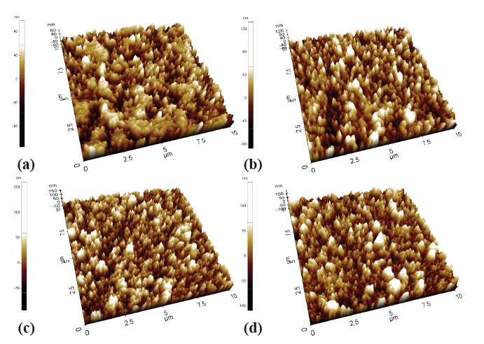
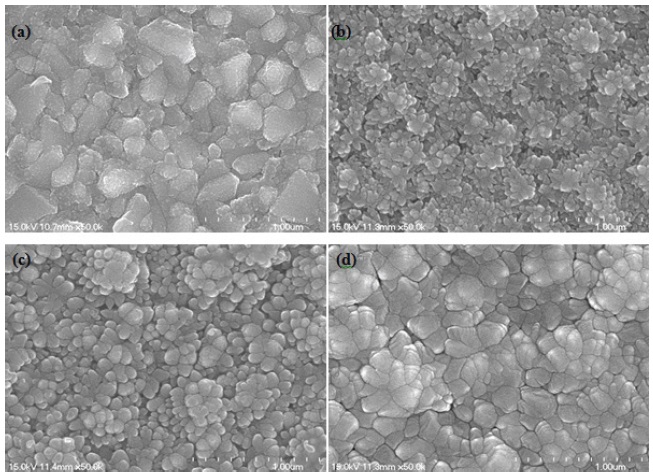
As shown in the FE-SEM image in Fig. 5 increasing RF-gun power, particle size was significantly bigger than low power. As power increases, the particle size increases [10]. From the surface of the 50 W gun power substrate, we can still observe the characteristic morphology of tin oxide crystals, since the thickness of ZnO film is relatively thinner and only approximately 105 nm. According to RF gun power, roughness of ZnO thin films was observed from the AFM shown in Fig. 4.
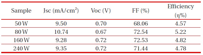
According to RF-gun power, passivating layers were observed with a thickness of 50 W 105 nm, 80 W 240 nm, 160 W 520 nm and 240 W 920 nm. We can see that the deposition rate of the ZnO passivating layer increased with increasing RF power, due to an increase in plasma density. Since the sputtering rate of Ar ions is critically dependent on the current density, which is applied to the cathode target, the sputtering rate of the ZnO passivating layer increased with increasing RF power [11]. Therefore, the 160 W and 240 W ZnO passivating layer transmittance dropped significantly (Fig. 6).
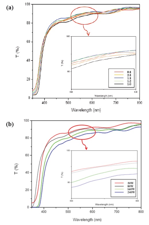
Figure 6(a) shows the transmission spectra of the FTO glass on the deposited ZnO films. The ZnO passivating layer sputtered at the Ar:O2 1:1 ratio showed identical transmittance of 90.11% at a wavelength of 550 nm compared to that of the bare FTO glass sample. Fig. 6(b) demonstrates that the optical transmittance of
the ZnO passivating layer, prepared on RF-gun power 50 W, was higher than the transmittance of other RF-gun power. With an increase in the sputtering power, ZnO Films thickness increased. According to the thickness, optical transmittances were decreased.
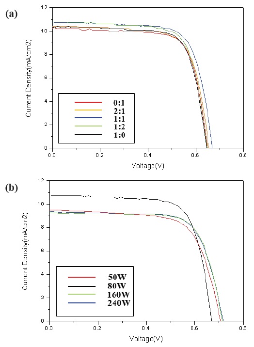
Figure 7 shows the photocurrent density - voltage (I-V) curves of the DSSCs with a ZnO passivating layer fabricated with different deposition rates, under 100 mW/cm2 illumination, in the AM 1.5 G condition. One of the most important parameters for a solar cell is its photoelectric conversion efficiency, i.e. the ratio of output power to incident power.
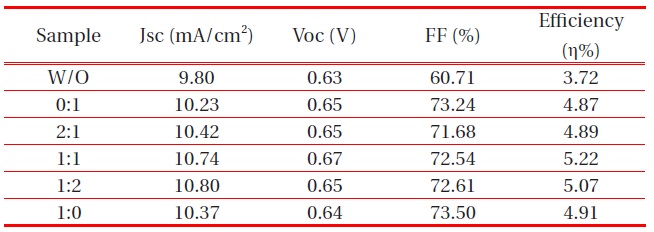
Solar cells with a high fill factor have a stable output voltage and current compared to cells with the same Voc and Jsc. Tables. 1 and 2 summarize the performance of the DSSCs fabricated. The DSSC using the ZnO passivating layer showed high conversion efficiency with a fill factor (FF) of 72.54%, a photocurrent density of 10.74 mA/cm2, an open circuit voltage (Voc) of 0.67 V, and a cell conversion efficiency of 5.22 %. However, the FF showed a growing trend, increasing from 60.71% to 72.54%, with a passivating layer. As a result, the highest conversion efficiency, η, was approximately 1.5% higher than the DSSC fabricated without a passivating layer. This was due to the strong effect of an energy barrier by blocking the electrons injected from the conductive
band of TiO2 to FTO substrate and the slight increase of transmission in the 550 nm wavelength. The optical transmittance of the ZnO passivating layer at the Ar:O2 1:1 ratio of 50 W was higher than other RF-gun power. However, the highest conversion efficiency appeared with 80 W gun power. We can surmise that the thickness of the ZnO passivating layer was optimized at 240 nm.

Effect of the ZnO passivating layer on the performance of DSSCs at different Ar:O2 ratios.
[Table 2.] Effect of the ZnO passivating layer on the performance of DSSCs RF-gun power.

Effect of the ZnO passivating layer on the performance of DSSCs RF-gun power.
In this study, properties of dye-sensitized solar cells, based on dense ZnO films deposited by RF magnetron sputtering, were examined. Optical results show that transmittance of ZnO passivating layers strongly depend on RF-gun power. Compared with the DSSC prepared without a passivating layer, the DSSC with ZnO passivating layers demonstrated a high fill factor and high conversion efficiency. The DSSC with the passivating layer, deposited under the 1:1 argon-oxide ratio, showed a high photocurrent density and a high fill factor (10.74 mA/cm2, 72%). The DSSC fabricated onto the FTO electrode with the ZnO passivating layer showed the highest conversion efficiency of 5.22% at an Ar:O2 ratio of 1:1, due to the prevention of the electron transfer to the electrolyte. Additional Ar:O2 ratios (1:0, 2:1, 1:2, 0:1) resulted in a decrease in efficiency and photocurrent density. Additionally, 80 W was the ideal RF-power. The improved conversion efficiency might be associated with improved surface roughness and transmittance of the passivating layer. The ZnO passivating layer coated TiO2 electrode has a promising application in the field of DSSCs, due to the fact that it provides effective prevention of recombination for electrons from FTO to electrolytes.