Semiconductor manufacturing operations include raw material supply, manufacturing systems, and finished products. Product applications for electronics are realized by chip manufacturers through industrial standards, production tools, materials and chemicals, metrology, and the technical workforce. Process control in semiconductor manufacturing has emerged as a crucial factor in creating cost-effective electronic manufacturing processes. Starting with statistical process control (SPC) in the 1980s, and continuing with computer integrated manufacturing (CIM) and advanced process control (APC), intelligent manufacturing systems (IMS) have consistently improved the quality of semiconductor products, as well as manufacturing effectiveness.
In integrated circuit (IC) manufacturing, the fabrication processes consist of several hundred sequential steps, and the potential yield losses that occur at every step cannot be ignored. The components of process control operations in leading-edge semiconductor manufacturing can be categorized as follows: 1) a run-to-run control basis (lot-to-lot or wafer-to-wafer control) at the lower level; 2) supervised control (tracking process by process) at a higher level; 3) a flexible manufacturing system resulting from powerful CIM concepts; 4) advanced
To accomplish reduced process variability, fault detection and classification (FDC) using tool data analysis and APC with
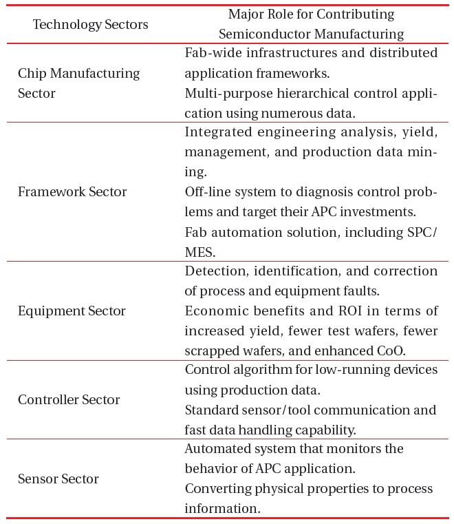
[Table 1.] Roles of Semiconductor AEC/APC technology sectors.

Roles of Semiconductor AEC/APC technology sectors.
sensors have arisen as urgent issues to be resolved [1-4]. Five sectors that contribute to the APC technology and their roles are listed in the Table 1.
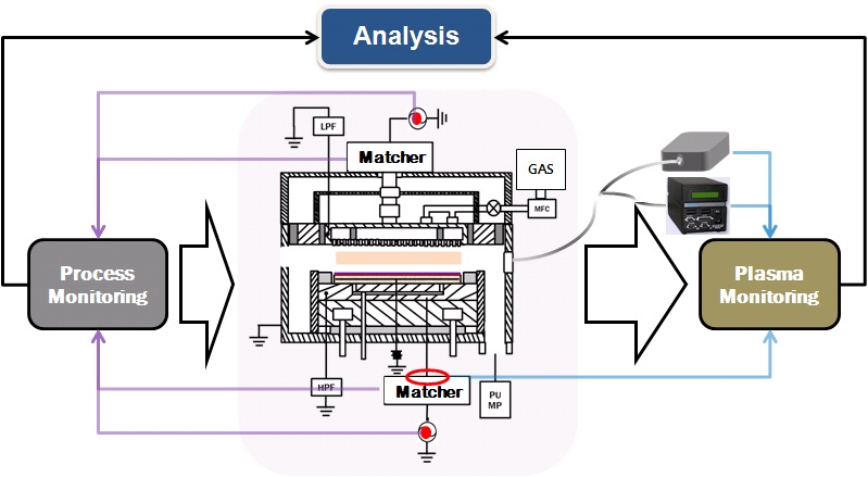
Among numerous semiconductor processes, plasma processing is one of the most important, with urgent requirements for real-time monitoring with advanced sensors. The monitoring and diagnosis of plasma etching started in the 1980s [5-7], and it is still a challenging topic in semiconductor process control. As allowable process margins continue to narrow, plasma monitoring techniques that include advanced
In this paper, the use of a chromatic monitoring method is presented for optical plasma process monitoring for the detection of process anomalies. Optical emission spectroscopy (OES), the most well-known plasma process monitoring sensor, provides high-dimensional plasma optical emission spectra, so dimensionality reduction or peak selection are always challenging. However, since the proposed optical monitoring system generates only three streams of red-green-blue (RGB) signals from a photo detector, high-speed optical data acquisition could be achieved that is as fast as current-voltage-type electrical sensors. Optical monitoring is non-invasive and is easy to install. Faster data acquisition enables the detection of extremely small perturbation, as short as hundreds of micro seconds. We report an observed abnormal plasma discharge as short as 210 μs.
2. SENSOR DEVELOPMENT AND EVALUATION
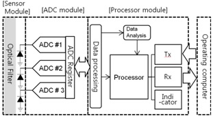
Add-on sensors for process monitoring should be able to accurately identify any suspicious behavior at its onset. Chromatic monitoring in plasma processing as a non-invasive method was previously proposed by Russel et al. [9]. In their study, a chromatic monitoring system provided significant speed advantages over the equivalent spectroscopic technique, optical emission spectroscopy (OES). The Plasma Eyes Chromatic System (PECS) is designed to observe the optical emission of a plasma glow discharge, and represent it with red-green-blue (RGB) values. The peak wavelengths of RGB are 620 nm, 540 nm, and 460 nm, with response ranges of 590-720 nm, 480-600 nm, and 400-540 nm, respectively. A schematic of the hardware configuration is presented in Fig. 1. Data collected in the master controller are converted from analog to digital, and the digitally processed signals are transferred to a PC for data visualization at up to 10 kHz, depending on the speed requirement in the application. The PECS is specifically designed to be compatible with a semiconductor manufacturing environment, and a graphical illustration of the
An initial experiment was performed to test the sensor response and correlate the optical data with process conditions. By modifying the process tool parameters, we investigated the relationship between the
under low chamber pressure. The brightness of the plasma color can also be varied depending on the amount of white components, and the combination of RGB is in white light emission.
Hue, saturation, and brightness (HSB) are aspects of color representation with red, green, and blue (RGB). All possible colors can be specified according to HSB, similarly to RGB, and visible light contains several light sources, whose energies are shown over a band of wavelengths. Hue (H) is the wavelength within the visible-light spectrum at which the energy output from a source is greatest. Saturation (S) is an expression for the relative bandwidth of the visible output from a light source, and it can be found by the size of the wavelength band of the light sources. As saturation increases, color appears more “pure,” and as it decreases, color appears more “washed-out.” Brightness is a relative expression of the intensity of the energy output of a visible light source. It can be expressed as a total energy value or as the amplitude at the wavelength where the intensity is great. Given a color defined by (
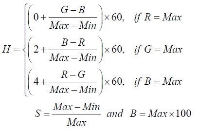
where Max and Min are the maximum and minimum values of (
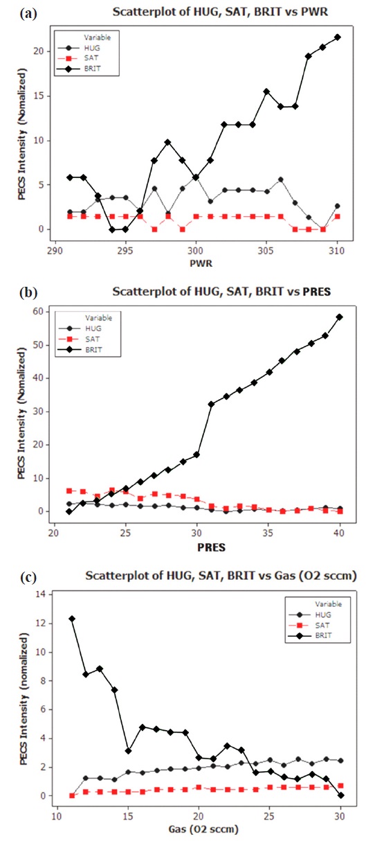
In Fig. 3, no obvious trends were found in hue and saturation, but a significant correlation was shown in brightness in response to changes in RF power, pressure, and gas flow. This experiment was performed without a wafer loaded in the chamber, so no byproduct would be observed. Thus, hue and saturation were not drastically changed. However, change in the process parameters affected the brightness of the detected optical emission. The increased RF power shown in Figure 3(a) increased the atomic/ molecular collision of plasma to generate higher optical intensities of all the sources of light. In the same manner, Fig. 3(b) reflects the increased possibility of atomic collisions from the decreased mean free path of the molecules in plasma. A monotonic decrease in brightness is interpreted as decreased total photon emission energy observed by the optical detector. When the chamber pressure is maintained at a certain level, the increased amount of oxygen gas will intensify the oxygen plasma, the color
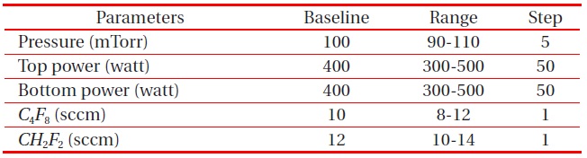
[Table 2.] Baseline process and ranges of variation.

Baseline process and ranges of variation.
of which is white, and it causes a reduction in its brightness. Therefore, the suggested optical monitoring method is useful for monitoring the change in plasma process conditions.
Employing an eight-inch (200 mm) production etching tool, five consecutive blanket oxide etch runs were performed while monitoring the plasma glow discharge using PECS. The etching tool used was an Exelan™ dielectric etcher manufactured
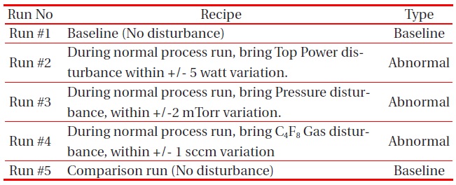
[Table 3.] Process fault scenario for the blind test.

Process fault scenario for the blind test.
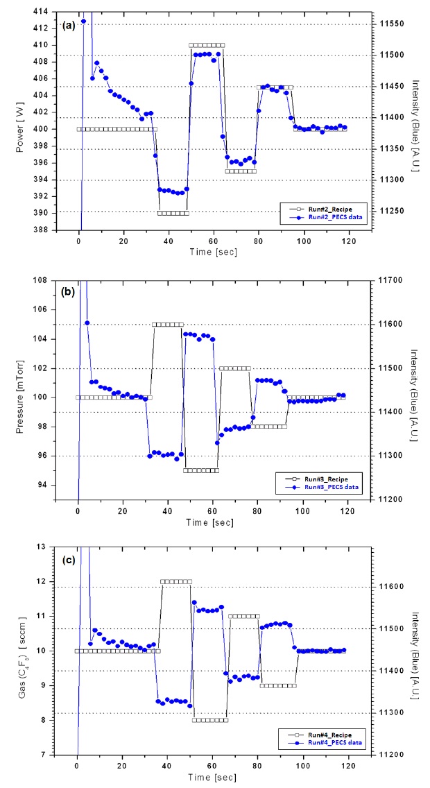
by Ram Research. The baseline process parameters and ranges are provided in Table 2. Each run lasted for one minute, and the process parameters were gradually modified every 10 seconds to quantitatively correlate the sensor response to process conditions.
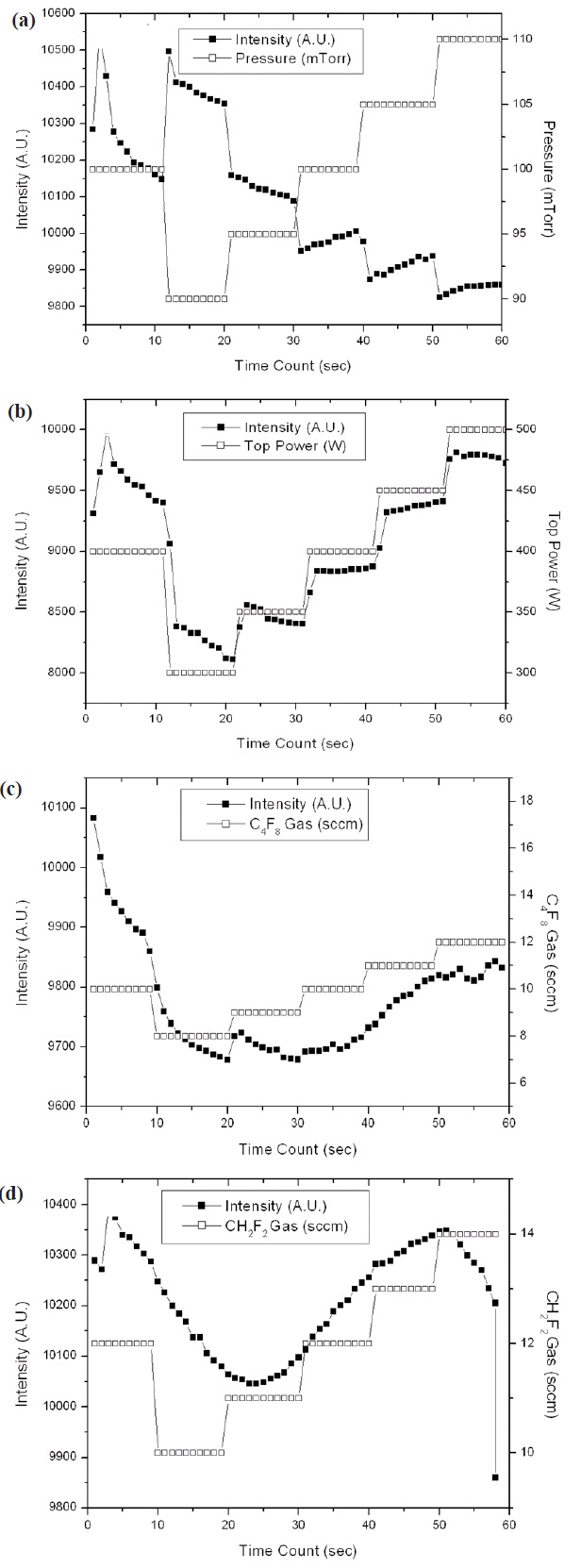
In Figs. 4(a)-(e), the sensor response is presented with respect to the process parameter modifications. As soon as the plasma was ignited, the optical response reflected the complicated plasma dynamics of dielectric breakdown in the gas phase. When the process was stabilized, the optical intensities measured by PECS followed the change in process parameters. For instance, when the pressure was increased (Fig. 4(a)), the sensor reading decreased. Absolute quantification of the pressure cannot be directly measured by PECS, but the relative deviation from the baseline can be quantified. The effect of power variation is also quite clear, as shown in Fig. 4(b).
However, more surprising was the fact that the optical sensor could detect changes in gas flow, as shown in Figs. 4 (c) and (d). Comparing these experimental results to the pressure and RF power variation shown in Figs. 4 (a) and (b), the acquired optical signals from the gas flow tracked the variation less accurately. The results seem to indicate that optical monitoring is less sensitive to gas flow compared with other process variables, but the rationale for slow tracking originated from the physical delay of gas delivery to the chamber. When the gas setting changes, there is an inevitable delay for the gas to be delivered to the chamber until the change is reflected in the plasma glow discharge. The delay depends on the length of the gas delivery line between the mass flow controller and the process chamber. Therefore, this optical signal is in fact also sensitive to the change in plasma glow discharge induced by the amount of gas flow change.
Following the affirming results presented above, we extended the investigation to explore a more realistic scenario for a manufacturing environment by examining small perturbations in process parameters. This experiment was performed with the same 200-mm tool, but the process parameters were not provided to us until the test was reported to the participating engineer (thus, a
baseline level for the remaining 20 seconds. In Fig. 5(a), of the baseline RF power was set to 400 watts , and perturbations of ±2.5% and ±1.25% were applied. For gas flow perturbation, ±1-2 sccm of
results are shown in Fig. 5(c). From the figures, it is evident that small perturbations of RF power, pressure, and gas flow change the state of plasma glow discharge. This can be detected by the PECS sensor, which can clearly serve as a signal indicator for detecting a faulty process.
It has been reported recently that plasma chamber arcing issues are of significant concern. Anomalous plasma discharge resulting in arcing is not yet monitored systematically, but it can make plasma conditions unstable, generate unexpected particles during the process, cause electrical damage to devices when the arc hits a metal contact opening or metal pattern in subsequent layers, burn or break wafers, or damage the electrostatic chuck in the etching system. One hypothesis for the cause of plasma arcing is the accumulated or unbalanced local discharge between the chamber and plasma or between the wafer and plasma. Noticeable arcs, called macro-arcs, can be easily detected in the form of sparks during the process or lightning marks after the process. Once this kind of arc takes place, the chamber must be
cleaned for the next process. However, we postulate that such a macro-arc is caused not by a single event, but by the accumulation of undetected micro-arcs. To avoid catastrophic failures that might cause wafer damage or unscheduled equipment maintenance, detecting micro-arcing during the process in real-time is crucial.
Previously, RF I-V probes have been suggested for arc detection, but such devices require hardware reconfiguration for the attachment of the sensor to the plasma tool. The specific mechanism of micro-arcing is still unknown, but it has been reported that plasma arcing is related to decreased electron density and increased electron temperature [10]. A practical approach to arc detection in a production environment is required, and we believe that this can be accomplished by detecting changes in plasma characteristics. Non-invasiveness is a high priority for real-time monitoring. In addition, to realize timely and accurate detection of arc events with durations of less than tens of microsecond, we propose the use of the PECS, a plasma monitoring system with 10-kHz data sampling rate capability. This frequency of data acquisition enables the detection of arcs of less than 10- ms duration, and optical monitoring via sidewall viewports in the etching system alleviate any concerns regarding intrusiveness and perturbation of the plasma or RF power that can result from the use of an external I-V probe.
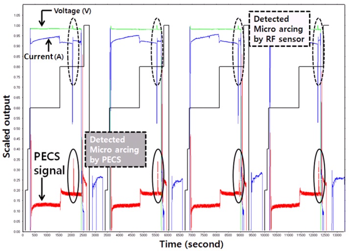
The experimental exploration of this approach consisted of 900 consecutive runs without a significant interrupt other than a prescheduled tuning and minor maintenance. Patterned silicon oxide wafers were etched in a 300-mm cluster tool for a production qualification test. An OES system and PECS were employed for
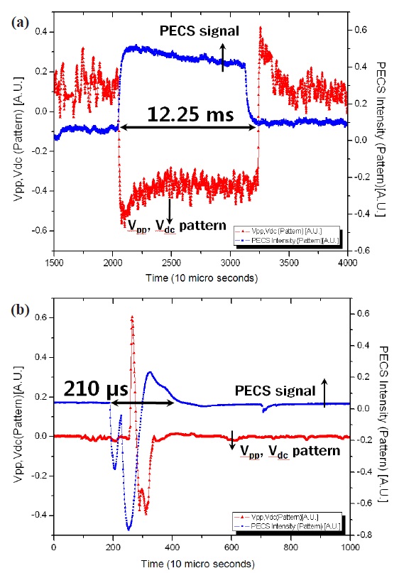
One of the test recipes consisted of a harsh environmental test, so that the possibility of chamber arcing was expected to be higher than under normal operation. As shown in Fig. 6, micro arcs were successfully detected in both the electrical and optical sensors. The amount of change in the electrical signal appeared to be significant, but the optical signal observed by PECS was more clearly noticeable. Detection occurred at identical points in both systems. While analyzing the detected arcs in Fig. 6, intensive discussions with process engineers were conducted to determine whether the signals represented true or false alarms. We have successfully detected several arcs during marathon tests, and other examples of detected arcs are presented in Fig. 7. Figure 7(a) shows a typical example for a relatively extended arc, and Fig. 7(b) shows the shortest arc that we observed.
4. LONG-TERM REAL-TIME PROCESS MONITORING
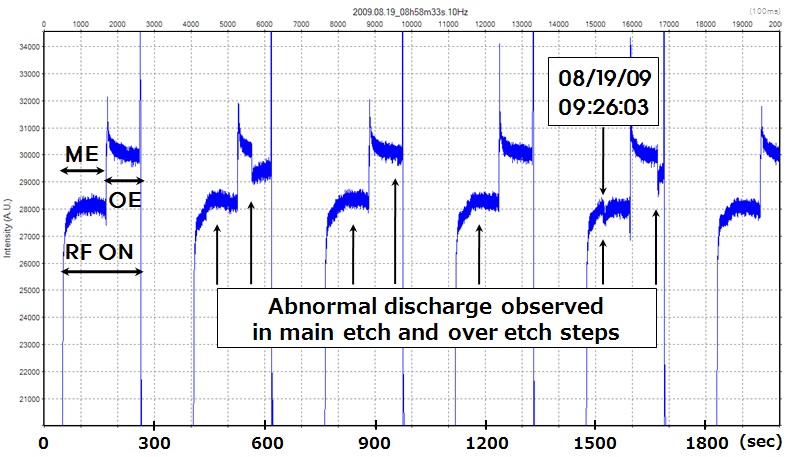
While developing a next-generation device fabrication process for high throughput and low plasma charging damage, realtime
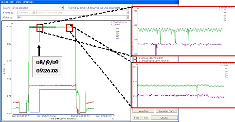
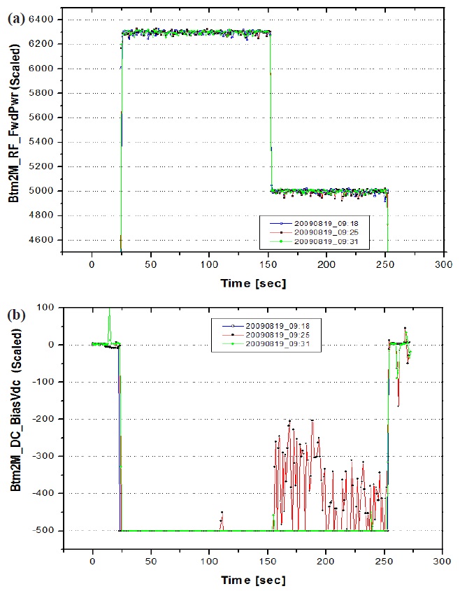
Simultaneous comparison of optical monitoring with the electrically detected abnormal discharge is presented in Figure 9. The abnormal discharge detected on 08/19/09 at 09:26:03 is shown in Figs. 8 and 9, but the suggested optical monitoring method observed the abnormal discharge or its symptoms in three wafers in advance comparing with electrical measurement. We also investigated tool data of the bottom electrode. Figure 10 (a) shows that no significant anomaly was observed in the Bottom
RF forward power in the corresponding three consecutive runs. However, the DC bias measured at the bottom electrode successfully detected such abnormal discharge. We postulate that the charge that continuously accumulated in the chamber was suddenly discharged by the accumulated electrical potential. When it was discharged onto the wafer or DC biased wafer chuck, it became noticeable at the bottom electrode, as shown in Fig. 10(b).
The PECS optical plasma process monitoring system has been introduced, and its application as a signal indicator for realtime process fault detection and as an arc detection system was explored. The development, verification, and adoption phase for the sensor system have been presented. The response of the PECS system was evaluated by modifying the process parameters (including RF power, chamber pressure, and gas flow) and observing the sensor behavior. PECS proved to be very sensitive to RF power changes, even allowing their quantification to some degree. Anomalies induced by the chamber pressure and gas flow variations were also observed. The system was also evaluated as an arc detection mechanism with promising results. Overall, the proposed PECS possesses great potential as a multi-purpose