Titanium nitride (TiN) has good diffusion prohibition, low electrical resistance, good thermal and chemical stability, and good adhesive property [1-4]. In addition, TiN has been considered as the most promised candidate to substitute for poly Si gate electrode, because poly Si gate electrode for the ultra thin gate SiO2 shows some problems of poly depletion through gate oxide and high resistivity [5,6]. For TiN gate electrode, it is possible to create fine patterns using high density plasmas, such as inductively coupled plasma (ICP), electron cyclotron resonance plasma (ECR), and helicon wave plasma. Until now, there have been a lot of papers on the etching of TiN thin film using halogen chemistries, such as Cl2/Ar, Cl2/N2, Cl2/HBr, Cl2/Ar/CHF3, CHF3/ Ar, SF6/Ar, and CF4/O2 [7-10]. But, reports on the etch mechanism of TiN thin film conflict with one another. Shamiryan
In this work, we investigated etching characteristics of TiN to SiO2, using an inductively coupled plasma (ICP) system. Etching characteristics were investigated in terms of TiN thin film, and selectivity of TiN thin film over SiO2 as a function of the etch chemistry. The chemical states on the etched surface were investigated with X-ray photoelectron spectroscopy (XPS).
TiN thin films were deposited by atomic layer chemical vapor deposition. The total thicknesses of the TiN thin films were about 100 nm. The dry etching process was performed in an ICP system [13], consisting of a cylindrical chamber with a diameter of 26 cm. The top copper coil was operated with 13.56 MHz RF power, and was located on the chamber lid to generate highdensity plasma. The bottom electrode was connected to another 13.56 MHz asymmetric RF generator, to control the DC-bias voltage. The distance between a quartz window and substrate electrode was 9 cm. The chamber was evacuated to 10-6 Torr using a mechanical pump (2M80, BOC Edwards), and a turbo molecular pump. The TiN thin films were etched with CF4/Ar gas mixing. The gas mixing ratio and process pressure were varied, to find the characteristics of etching. For these experiments, RF power, DC-bias voltage, process pressure and substrate temperature were 700 W, - 150 V, 15 mTorr and 45℃, respectively. In addition, plasma etching of TiN thin films was investigated by including the RF power, DC-bias voltage, and process pressure of 500 W ~ 650 W, - 150 V ~ - 300 V, and 9 ~ 20 mTorr in the CF4/Ar gas mixing ratio, respectively. The etch rates were measured using a depth profiler (KLA Tencor, α-step 500; Sanjoe, Ca, USA). The chemical reactions on the surfaces of the etched TiN thin films were evaluated using X-ray Photoelectron Spectroscopy (XPS, Thermo VG, SIGMA PROBE; East Grinstead, West Sussex, England). The source type for the XPS analysis was Al Kα with a spot size of 400 μm. The energy step size was 0.1 eV.
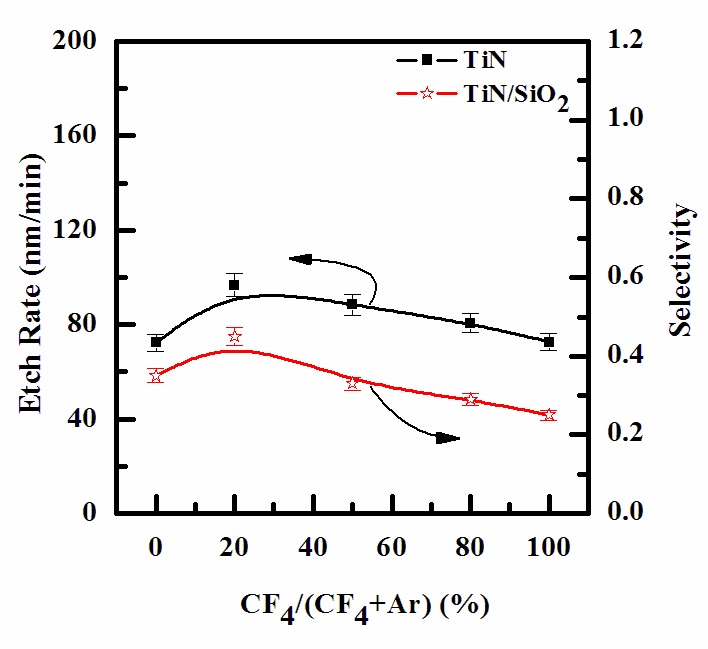
For the characterization of TiN thin film in a ICP etching system, the plasma etching of TiN thin film and selectivity of TiN to SiO2 were systematically investigated as various etch chemistries. Figure 1 shows the etch rate of TiN thin film, and selectivity of TiN to SiO2 as a function of reactive species concentration, when the total flow rate was maintained at 20 sccm. Other process conditions, such as RF power, DC-bias voltage, process pressure, and substrate temperature, were maintained at 700 W, - 150 V, 15 mTorr, and 45℃, respectively. Comparisons of etch rates of the TiN thin film in Ar- (72.5 nm/min) and CF4- (72.7 nm/min) based plasmas showed that the chemical etching was more effective than the physical sputtering. The etch rate of TiN thin film increased, while the selectivity of TiN to SiO2 paralleled. The result was a lowering of the rate of the chemical reaction in the CF4 plasma, due to the deposition of solid inorganic compounds that resulted from a complete dissociation of the CF4 molecules. The maximum etch rate of TiN was 96.7 nm/min at a 20 % of CF4/ (CF4+Ar) gas mixing ratio. It was well known that fluorine components of TiN thin film form high-volatile by-product, such as TiF4 (melting point: 284℃). The evident enhancement of the TiN thin film etch rate in the pure CF4 plasmas allows one to assume that the chemical etch pathway provided by the F atom is the dominant mechanism for the given set of process parameters. In the case of the chemical etching of the TiN thin films, we expect the contribution of this pathway to be much lower, compared with the chemical reaction. In CF4-based plasma, addition of the CF4 up to 20% increased the etch rate, through the action of two mechanisms: 1) the accelerated chemical reaction by the ionstimulated desorption of the reaction products, and 2) increasing of the contribution of the chemical etching. Nevertheless, when the CF4 content exceeds 20%, the etch rate begins to fall, down due to the “disappearance” of the chemical etching [11,12].
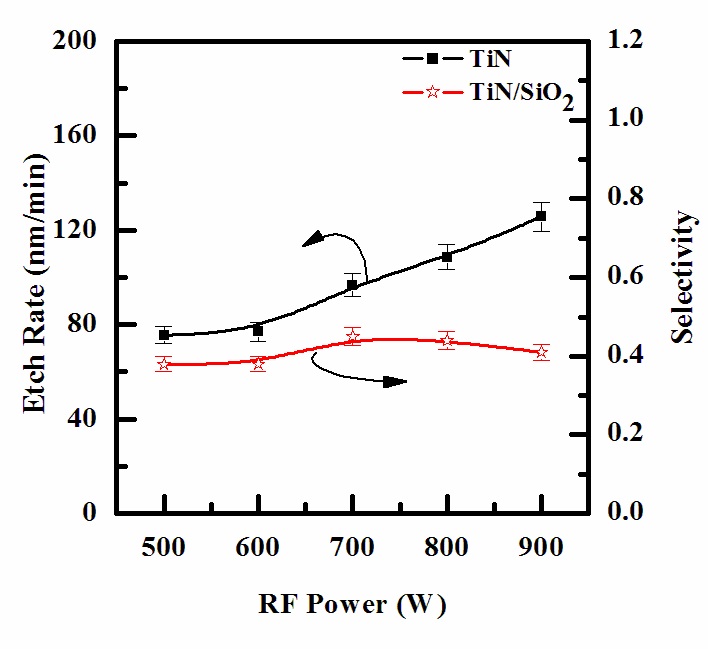
Figure 2 shows the etch rate of TiN thin film as a function of RF power. Other process conditions, such as CF4/Ar (20:80%) plasma, DC-bias voltage, and process pressure, were also maintained at - 150 V, and 15 mTorr, respectively. As the RF power increases, the TiN thin film also increases, starting from 75.7 nm/ min at 500 W, and then reaches a maximum of 125.7 nm/min at 900 W. It can be seen that an increase in the RF power causes a
monotonic increase in both dissociation and ionization rates, and thus in densities and fluxes of F atoms and positive ions. In our case, such layer can result from the deposition of solid F that is then bonded with surface oxygen to form Ti-F, as well as from F radicals incorporated in the polymer-like structure.
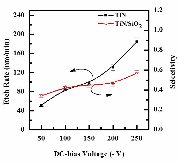
The etch rates of TiN thin film are shown in Fig. 3 as functions of DC-bias voltage. Other process conditions, such as CF4/Ar (20:80%) plasma, RF power and process pressure, were also maintained at 700 W, and 15 mTorr. As the DC-bias voltage increased from - 50 to - 250 V, the etch rate of TiN thin film increased from 51.5 to 184.5 nm/min. The selectivity of TiN to SiO2 slightly increased. An increase in etch rate can be related to the increase of mean ion energy, resulting in increasing sputtering yields for the TiN thin film and reaction products.
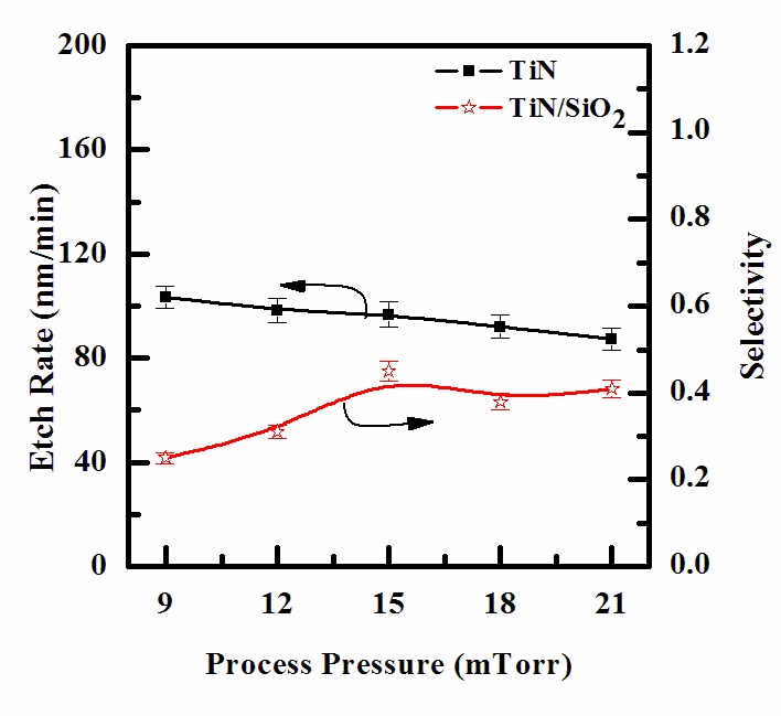
The effect of process pressure on etch rate is shown in Fig. 4. As process pressures increased from 9 to 21 mTorr, the etch rates of TiN decreased from 103.8 to 87.4 nm/min. However, we obtain a similar non-monotonic behavior, as was mentioned for the effect of the gas mixing ratio. In our opinion, the effect of gas pressure can be explained as follows: an increase in gas pressure at fixed CF4/Ar mixing ratio leads to an increase in both density and flux of fluorine atoms on the etched surface, but causes a decrease in ion flux and mean ion energy [13,14]. As a result, with increasing gas pressure, we have a tendency to accelerate in the chemical etch pathway, but a worse condition for the ion
stimulated desorption of reactive products obtains, resulting, probably, in a decreasing fraction of acceptable free surface for chemical reaction. Similar to the effect of the gas mixing ratio discussed above, these two factors, working in opposite directions, produce a non-monotonic behavior of the etch rate.
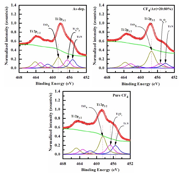
For more detailed investigations of the chemical reaction between TiN and fluorine atoms, XPS analysis was performed. In order to determine this in detail, XPS narrow scan analysis was performed as a function of CF4 content in CF4/Ar plasma. Figure 5 shows narrow scan spectra for Ti 2p from TiN surfaces. As shown in Fig. 5 (a), the Ti 2p corresponded to TiOx (458.65 eV), TixOy (456.5 eV), and Ti-N (455.25 eV) bonds, and after the TiN was exposed in CF4/Ar (=20:80%) plasma, three peaks corresponded to TiOx bond (457.45 eV), TixOy bond (455.3 eV) and Ti-N bond (454.05 eV). The bonds from TiN thin film may exist at a lower binding energy of 1.2 eV. As shown in Fig. 5(c), the TiOx, TixOy, and TiN bonds existed at the higher binding energy of 0.3 eV. This indicates that the TiN surface was changed by ion sputtering and the formation of etching byproducts.
Figure 6 shows narrow scan spectra for N 1s from TiN surfaces. In Fig. 6(a), the peak is observed at 396.8 eV. The N 1s peak corresponded to the peak at 397.05 eV, and 395.95 eV corresponded to the N-Ti bond or N-Si bond. As shown in Fig. 6(b), the N 1s peak decreases and N-Ti and N-Si peak increases and a new peak appeared for the N-F bond (401.7 eV). Also, the N-Ti and N-Si bond
from N 1s may exist at a lower binding energy of 0.85 and 1.6 eV at 397.05 and 395.95 eV. In Fig. 6(c), the N-Ti and N-Si peak also decreased after etching in pure CF4 plasma, compared with Fig. 6(a). This indicated that N can be effectively removed by forming etch byproducts, such as N-Ti bond.
XPS analysis confirmed this. The etch rate behavior of TiN in CF4/Ar(20:80%) can be explained as follows; 1) N can be effectively removed by formation of volatile etch byproduct N-F. 2) The byproduct can accumulate on the TiN surface. The byproduct prevents further chemical reaction between the CF or F radical and the TiN layer. 3) The byproduct can be removed by Ar ion sputtering. The low etch rate in pure CF4 plasma is related to the formation of byproduct. This assumption is in good agreement
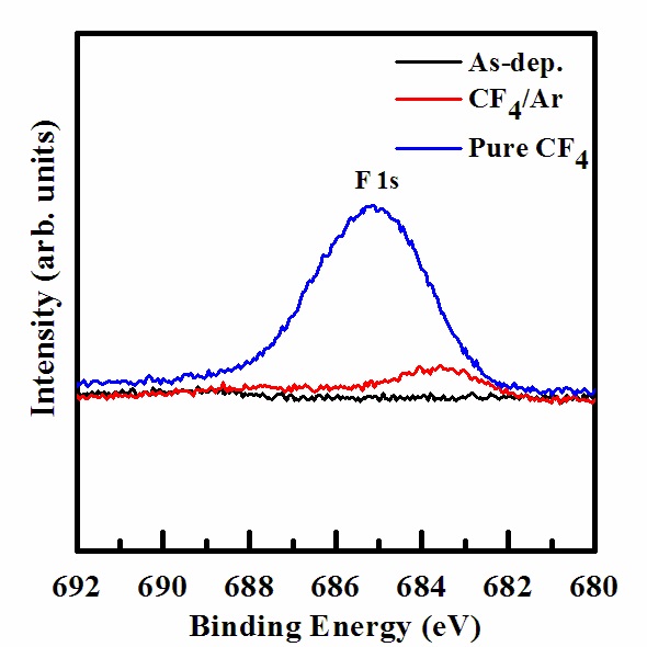
with the etch rate behavior of TiN, as discussed in Figs. 2-5. The F 1s peaks are shown in the spectrum of Fig. 7, which was obtained from the etched sample. The photoelectron binding energy of 685.2 eV was assigned to F 1s, resulting from the less volatile TiFx, leading to an increased etch rate with increasing amount of CF4. When the TiN thin films were etched in the CF4/Ar (20:80%) and pure CF4 plasmas, the F 1s peak intensity decreased, owing to the F atoms from CF4 gas [15-17].
Etching characteristics of TiN thin films were investigated in terms of etch rate and selectivity, using CF4/Ar plasma. Experiments were performed with variations of CF4/Ar gas mixing ratio, RF power, DC-bias voltage, and process pressure. It was found that addition of CF4 contents up to 20% led to the etch rate of TiN decreasing, in comparison with at CF4 only. The maximum etch rate of TiN films was 96.7 nm/min under 20% CF4/(CF4+Ar) in 700 W, - 150 V, 15 mTorr, and 45℃. This showed that the increase of CF4 addition enhanced ion bombardment, and made the etch rate decrease. The chemical states of etched TiN films were investigated using XPS, and the chemical reaction between TiN and F was observed. The etching mechanism of TiN thin films can be explained as follows: Ti interacted with the F radical by adding CF4, but non-volatilie etch byproducts such as TiFx remained at the surface.