In order to improve the price competitiveness of semiconductor chips, the semiconductor market has recently required high performance, size reduction, and low unit prices. To this end, however, a great deal of investment costs and time are required, from the development of new high-performance semiconductor products, to their mass production. To improve product competitiveness, reduction in production costs and time is emerging as an important task. The overall semiconductor fabrication process is segmented into the processes of chip production on the wafer, testing, and packaging. While the production costs and period for semiconductors have greatly been reduced due to the investment in manufacturing facilities and the development of new processes, technologies for the testing process at the wafer level have not kept pace with the speed of cost and time reduction. A probe card with a plurality of probes is an important component, which electrically connects semiconductor devices on the wafer with a semiconductor test system that tests whether the devices are defective or non-defective, prior to the packaging process. The probe card is increasingly of more and more importance [1-3]. As memories show increasingly higher levels of performance, and system large scale integrated circuit (LSI) devices offer increasingly higher densities, the sizes of semiconductor devices are relatively decreasing, resulting in reduced pad sizes, and fine pitches between pads [4,5]. Therefore, test systems to judge whether integrated circuit (IC) chips on a wafer are nondefective or defective also need to be developed rapidly, in line with semiconductor development technologies. Accordingly, fabrication technologies for probe cards that connect electrical signals between a test system and wafers are core technologies in the semiconductor testing process [6,7].
Probe cards can be classified into conventional cantilever-type, based on the horizontal array of probes by bending the ends of probe tips, the vertical type, based on the array from standing probe tips vertically [4,5,8,9], and the MEMS type, which forms probe tips by using micromachining technologies [10-13]. Until now, conventional cantilever-type probe cards have frequently been used, which are fabricated manually. However, as semiconductors have achieved high levels of integration over recent years, the pitches of the input and output pads of semiconductor chips have continued to decrease. Moreover, according to the progress in the development of system on chip (SoC) devices, probing technologies that can accommodate the complexity of the devices also need to be developed. Accordingly, the development of vertical (1.5 generation) or MEMS (2nd generation) probe cards is accelerating beyond that of conventional cantilever probe cards (1st generation) [13-15]. Conventional cantilever-type probe cards have the structure in which the ends of probe tips are bent, and thousands of probes are arrayed to fit the locations of chip pads. In order to fix the tension between probe tips at a certain level, probe tips with different thicknesses are used. However, if the number of test pads increases and the pitch between probe tips is reduced for high-density tests, distortion of probes can occur during a chip test. This distortion can easily cause a short with adjacent probes and leakage currents. For such reasons, it is difficult to perform multi-chip tests and high-frequency tests. In addition, as conventional cantilever-type probe cards require the molding of epoxy probes, these have the disadvantage that the repair of probe pins is impossible. Therefore, to overcome the problems of existing horizontal cantilever-type probe cards and realize high-density tests, the development of vertical and MEMS probe cards is actively underway. Vertical probe cards are more advantageous in tests of semiconductor devices with areaarray pads, and more convenient for the repair of probe pins. But, large pitches between the probe tips make these cards unsuitable for the tests involving applications to various semiconductor devices [4,5]. However, MEMS probe cards can be fabricated using variously shaped probes, which are made by MEMS process. Therefore, despite their high costs, MEMS probe cards have high levels of mechanical reliability and electrical characteristics, leading to their use in a wide range of fields, including memory [10-13], as the MEMS process can fabricate various shapes of probes with different application types. In addition, as the technologies realize shorter diameters and lengths compared to conventional tungsten probes, these have outstanding signal characteristics. In particular, with the utilization of MEMS technologies, probe cards can be made at the wafer level. As a result, test time and costs can be dramatically reduced, compared to existing manual assembly technologies, and superb performances can be derived, in terms of the accuracy of tips, and repeated tests. In addition, as the technologies can conduct prompt and reliable device tests in response to new packing methods, probe card fabrication technologies using the MEMS process are considered essential [16,17].
The present study proposed a fabrication process technology for simple and low-price three-dimensional cantilever-type MEMS probes that can test DRAM chips at the wafer level. For the fabrication process for low-price probes suited to large areas, conventional MEMS techniques, such as wet anisotropic etching, dry etching, metalizing, electro-plating, and bonding, were used on a silicon substrate. Finally, the mechanical and electrical characteristics of the fabricated probes, in terms of leakage current, contact resistance, planarity and
2. DESIGN AND FABRICATION OF MICROPROBES
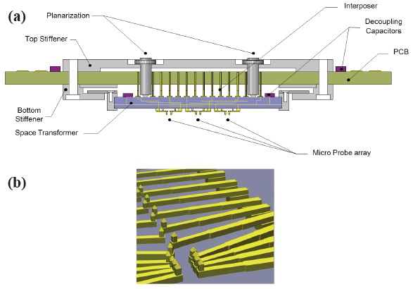
Figure 1(a) shows a schematic diagram of a conventional probe
card. A conventional probe card is composed of microprobe arrays, a ceramic space transformer, top stiffener, bottom stiffener, PCB, and interposers that electrically connect the PCB and the space transformer, as well as act as a spring for planarization of a probe card. Figure 1(b) is a magnified image of the microprobe arrays. In general, they should be designed to have an overdrive of 100 μm at 4 gf contact force, and displacement up to the overdrive of 150 μm. In terms of design, probe beams and probe tips were designed to withstand 150 μm or higher overdrives, through cantilever-related formulas and simulations [9].
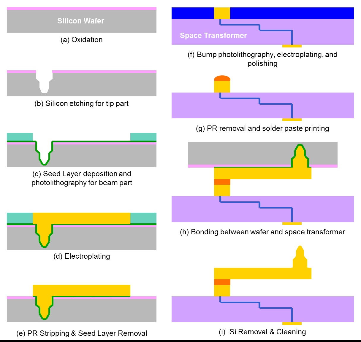
The fabrication process for a cantilever-type MEMS probe card with its microprobes is shown in Figure 2 [8,9]. The substrate for the fabrication of the probes was a 6-inch, p-type, (100) silicon wafer, with thickness of 650 μm. After initial cleaning, a 1 μmthick wet thermal oxidation film was grown on a silicon wafer (Fig. 2(a)). Thereafter, the oxidation film was etched through the photolithography process, using a GXR601 photoresist and the reactive ion etching (RIE) method. A part of each microprobe tip was formed through dry etching with the deep reactive ion etching (DRIE) method, while employing the etch window opening formed as an etch mask for silicon. The conditions for the DRIE process used in the dry etching of silicon are shown in Table 1. Thereafter, the pointed shape of the probe tip was completed through wet etching with potassium hydroxide (KOH) solutions (Fig. 2(b)). Using a sputtering method, titanium (Ti) and copper (Cu) were deposited with the respective thicknesses of 50 nm and 300 nm, to form the seed layers. After this, the shape of a probe beam was built using a THB-151N photoresist on the Cu seed layer (Fig. 2(c)). Thereafter, according to the electro-plating conditions in Table 2, each microprobe was plated with nickelcobalt (Ni-Co) alloy, and then polished to the thickness of 60 μm (Fig. 2(d)). With the removal of the photoresists and seed layers, the fabrication process for probes on the wafer was completed (Fig. 2(e)). In order to define bumps on the space transformer, photolithography process was conducted using photo-sensitive dry film. The photo-sensitive dry film with a thickness of 250 μm was laminated on the space transformer using a vacuum laminator. Then the patterns were defined by conventional exposure, and developing process. Subsequently, nickel (Ni) was electroplated in dry film mold, and polished to 200 μm (Fig. 2(f)). To make arrays of the probes on the space transformer, a bonding process is essential. In this study, gold-tin (Au-Sn) paste was used as the solder materials for bonding. Using a screen printing process, a gold-tin paste was patterned on the area of the space transformer, to which probes will be bonded (Fig. 2(g)). Thereafter, the wafer and the space transformer were bonded using a flip-chip bonder at a temperature of 300℃ (Fig. 2(h)), and then,
[Table 1.] DIRE process conditions for the microprobe tips.
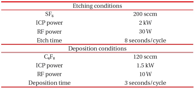
DIRE process conditions for the microprobe tips.
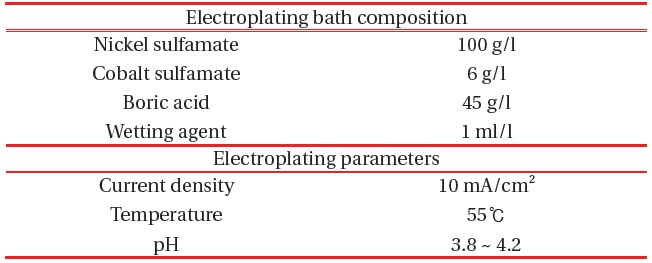
[Table 2.] Ni-Co electroplating bath composition and parameters.

Ni-Co electroplating bath composition and parameters.
as the final step, the silicon substrate and the seed layers were all removed in KOH solutions (Fig. 2(i)). In this paper, we reduced several process times and consumable materials compared to the previous developed MEMS probes [10]. We reduced one DRIE process of the fabrication steps for probes on the wafer. In addition, another sacrificial silicon wafer, including photolithography, DRIE, oxidation, and ceramic bonding processes, was essential in previous study for bump fabrication on the space transformer. However, a series of expensive processes and another sacrificial silicon wafer were replaced with a conventional dry film lithography method in our study, using thick photo-sensitive dry film and vacuum laminator. By reducing the fabrication steps and consumable materials in this research, we developed more highly productive process technologies for MEMS probes than others.
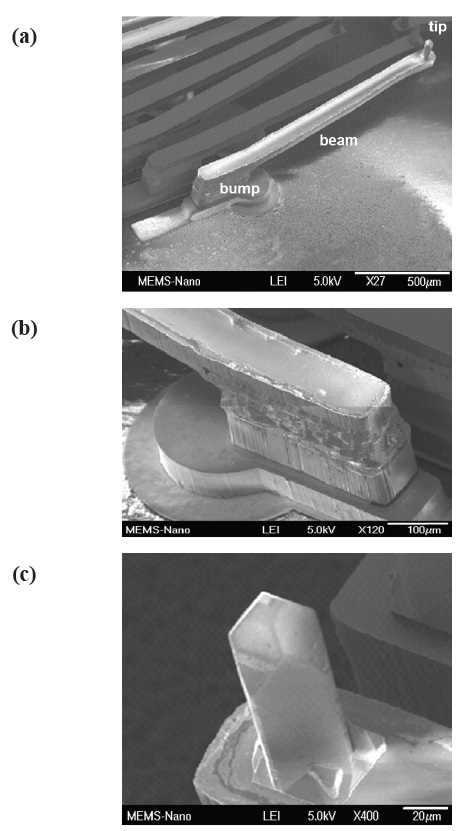
Figure 3(a) shows a SEM image of a microprobe composed of a tip, beam, and bump. Figure 3(b) is a magnified image of the bonding area between microprobes and the space transformer. This shows that the probe and the bump are well bonded by the Au-Sn alloy solder, and accurately arrayed. Figure 3(c) is a magnified image of the probe tip, showing that a pyramid shape is accurately formed.
The space transformer with microprobes is combined with the PCB, in order to measure the
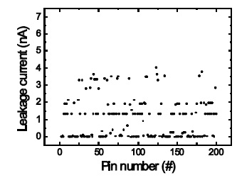
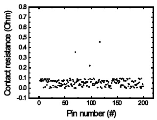
also revealed an average leakage current of around 1.04 nA, and an average contact resistance of 0.054 Ω. These measured values satisfied the specifications of the probe card to measure DRAM chips.
In the present study, cantilever-type microprobe arrays for the measurement of DRAM chips were fabricated, and their mechanical and electrical characteristics were analyzed. The microprobe arrays were fabricated using a conventional MEMS process with manufacturability, and a Ni-Co alloy was used as their materials. An Au-Sn paste was used for the bonding of the probes fabricated with the space transformer. Final probe arrays were completed by completely removing silicon after the bonding. The electrical and mechanical characteristics of the fabricated probes were measured by combining the space transformer with the microprobe arrays and the PCB. The