Due to a high optical transparency and an efficient conductivity, transparent conductive oxide (TCO) materials have widely been used as electrodes or semiconductors for electro-optical devices, such as solar cells, and flat panel displays (FPD). Indium tin oxide (ITO) has been used as a transparent pixel electrode in FPDs such as thin film transistor liquid crystal displays (TFTLCD), or active matrix organic light emitting diodes (AMOLEDs) [1,2]. Indium gallium zinc oxide (IGZO) has attracted much attention for use as an active layer in TFTs, because of its high mobility [3,4], and zinc oxide (ZnO) has been used as a semiconductor in sensor applications and solar cell technology [5,6]. For application to electrical devices, it is necessary to pattern TCO layers in the fabrication process. For a long time, TCO patterns have been obtained by using photolithography and chemical wet etching. However, the process itself consists of at least 7 unit process steps, including photoresist coating, ultraviolet (UV) exposure, and various chemical reactions and heat treatments [7]. Moreover, the process creates chemical waste from the developers, wet etchants, and photoresist strippers used which incur high costs for their disposal. Therefore, new patterning methods have been used for the simple patterning of TCOs [8,9]. Laser direct patterning has been used to reduce the number of process steps to one [10,11].
In this work, a Q-switched diode-pumped neodymium-doped yttrium vanadate (Nd:YVO4, λ=1,064 nm) laser was used to pattern ITO, IGZO, and ZnO films on slide glass substrates, and the laser ablation results were investigated and compared. For various laser beam conditions, the ablated results were analyzed while considering the effect of the structural characteristics of various TCO films on the direct patterning.
ITO, IGZO, and ZnO were sputtered at room temperature to a thickness of 500 Å on slide glass substrates. ITO film was deposited by DC sputtering at a power density of 1.8 W/cm2, with a gas
mixture of Ar 50 sccm and O2 1.5 sccm. IGZO film was deposited by RF sputtering at a power density of 0.64 W/cm2 and Ar 50 sccm. ZnO film was also deposited by RF sputtering at a power density of 1.2 W/cm2 and a gas mixture of Ar 50 sccm and O2 1.5 sccm.
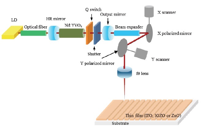
Figure 1 shows the experimental setup for the laser ablation of various TCO films on slide glass substrates. The laser system was a diode-pumped, single-mode, Q-switched Nd:YVO4 solid-state laser with a wavelength of 1,064 nm, a pulse duration of τ = 10 ns full width at half maximum (FWHM), and a pulse repetition rate of 0~200 kHz. The laser beam was scanned by a galvanometric beam scanning system, and de-magnified across the sample area of 100 mm × 100 mm using an F-theta lens with a focal length of 160-mm.
Laser ablation was carried out at three different pulse repetition rates (40, 60, and 80 kHz) and four different scanning speeds (100, 500, 1,000, and 2,000 mm/s). Laser ablation was performed a total of 12 times on each TCO sample. After laser ablation, the morphologies of the scribed patterns were observed using a scanning electron microscope (SEM, Hitachi S-4700). Furthermore, the etched depths and the roughness of the scribed grooves were investigated by a stylus profilometer (KLA TENCOR, alpha-step 500).
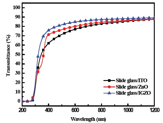
The transmittances of TCOs were measured using anultraviolet/ visible/near-infrared light (UV/Vis/NIR) spectrometer (LAMBDA 750). As shown in Fig. 2, the IGZO film shows a much higher transmittance of 88.72% at 1,064 nm than ZnO (87.08%) and ITO (86.49%) films.
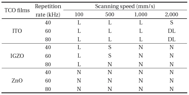
The laser ablations in different laser beam conditions resulted in different scribed grooves on the samples, as shown in Table 1. It is observed that most of the laser beam (except at the speed of 2,000 mm/s) caused a continuous scribed line on ITO film. In the case of the IGZO film, continuous scribed lines were obtained for only a low scanning speed (100 mm/s). It was also possible to find a discontinuity of the scribed line, or spots instead of a continuous line when the scanning speed was increased. At scanning speed higher than 500 mm/s, the IGZO film was not removed by the laser ablation. It is thought that the laser beam cannot be concentrated on the film with the sufficient energy to etch the IGZO film when the scanning speed is high. As for the ZnO film, it was impossible to find the scribed patterns for any laser beam condition. It is thought that the binding energy of ZnO is so high that the laser beams could not affect the film.

TCO films laser ablated at various laser beam conditions. L, DL, S, and N represent “line”, “discontinuous line”, “spot”, and “none”, respectively.
For the etching of the laser scanned parts of the films, the laser beam should have enough energy to melt and remove the film, and the transient thermoelastic stress produced by rapid laser heating should exceed the fracture limitation of the film [12]. The energy of the laser beam and the energy absorbed by unit area of the films were influenced by the laser beam conditions of repetition rate and scanning speed, respectively. The etched depths and the roughness of the scribed grooves were investigated and analyzed. The etched depths were about 500 Å, and the ITO and IGZO films were almost all removed in all of the laser beam conditions.
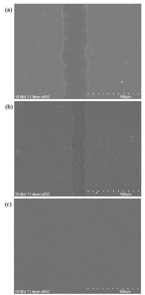
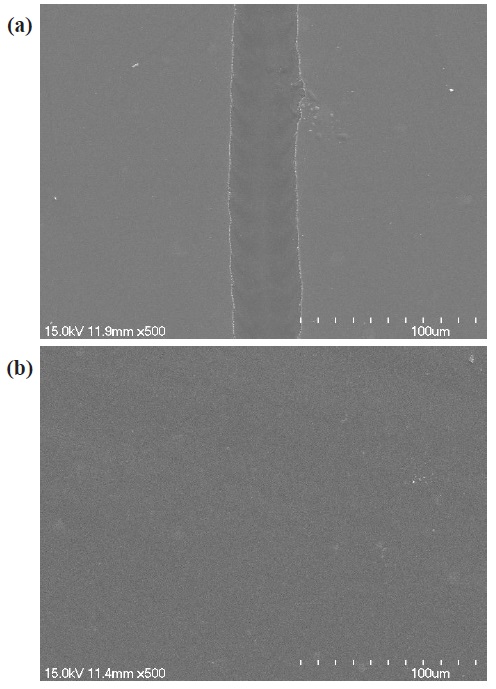
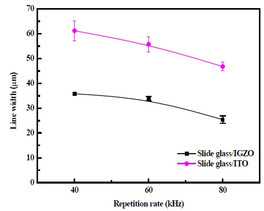
The SEM images of laser-ablated films are shown in Fig. 3 (at 100 mm/s and 80 kHz) and Fig. 4 (at 1,000 mm/s and 60 kHz). In Fig. 3(c), it was impossible to find the scribed patterns for any laser beam conditions on the ZnO film. In the case of the IGZO film, continuous scribed lines were obtained for only low scanning speed (100 mm/s), as shown in Figs. 3(b) and 4(b). It is worth noting that the laser-ablated ITO lines were wider than the laser-ablated IGZO lines. When the repetition rate was changed from 40 kHz to 80 kHz for the scanning speed of 100 mm/s, the line width of the laser-ablated IGZO patterns was decreased from 35.82 μm to 25.37 μm. However, the line width of the laserablated ITO patterns was changed from 61.19 μm to 46.77 μm, as shown in Fig. 5. The line widths of laser-ablated patterns were decreased when the repetition rate and the scanning speed increased. This is attributed to the non-uniform distribution of the intensity of the laser beam spots, which were formed on the film when each pulse of the laser beam passed through the F-theta lens (as shown in Fig. 1). The ablated line width was decreased from 61.19 μm to 36.32 μm when the scanning speed was increased from 100 mm/s to 2,000 mm/s at a repetition rate of 40 kHz. The result is related to the overlapping of the unevenly distributed
[Table 2.] The element atomic percentages of TCO films determined by XPS.
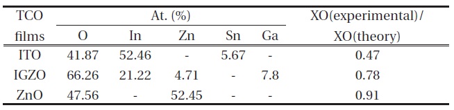
The element atomic percentages of TCO films determined by XPS.
laser beam spots.
For the analysis of the dependence of the TCO film on the laser ablation patterns, X-ray photoelectron spectroscopy (XPS) was used for investigation of the structural characteristics of the TCO films. The element atomic percentages of TCO films are shown in Table 2. This table also contains the experimental values and theoretical estimates of the oxygen content ratios. For ITO, IGZO, and ZnO films, the theoretical estimate of the oxygen content is obtained by equations (1), (2), and (3), respectively.


Where
A Q-switched Nd:YVO4 laser (λ=1,064 nm) was used to ablate various TCO films such as ITO, IGZO, and ZnO films on glass substrate. The laser ablation results showed that ITO film was fully etched for all the laser beam conditions. ZnO film was not etched for any conditions, and IGZO film was etched for only a lower scanning speed of the laser beam. The difference is thought to have come from the ZnO and IGZO films having lower CTE values and higher binding energies than ITO film.