Plasma etching of high-
Research to date shows the dependence of the ZrO2 etch rate on the operating conditions, using Cl2/Ar, HBr/CF4, and HBr/SF6 plasmas, but does not discuss the etch mechanism, the relationships between the process parameters, or the chemistry.
In this work, we investigated the etching characteristics of ZrO2 to SiO2, using an inductively coupled plasma (ICP) system. Etching characteristics were investigated in terms of ZrO2 thin film, and selectivity of ZrO2 thin film over SiO2 as a function of the etch chemistry. The chemical states on the etched surface were investigated with X-ray photoelectron spectroscopy (XPS).
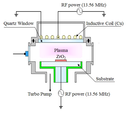
The ZrO2 thin films used in this work were deposited by atomic layer chemical vapor deposition. The total thicknesses of the ZrO2 thin films were about 100 nm. The dry etching process was performed in an ICP system, as shown schematically in Fig. 1. This consisted of a cylindrical chamber with a diameter of 26 cm. The top copper coil was operated with 13.56 MHz RF power, and was located on the chamber lid, to generate high-density plasma. The bottom electrode was connected to another 13.56 MHz asymmetric RF generator, to control the DC-bias voltage. The distance between a quartz window and the substrate electrode was 9 cm. The chamber was evacuated to 10-6 Torr using a mechanical pump (2M80, BOC Edwards) and a turbo molecular pump. The ZrO2 thin films were etched with CF4/Ar gas mixing. The gas mixing ratio and process pressure were varied, to find
the characteristics of etching. For these experiments, RF power, DC-bias voltage, process pressure and substrate temperature were 600 W, - 250 V, 15 mTorr and 45℃, respectively. In addition, plasma etching of ZrO2 thin films was investigated by including the RF power, DC-bias voltage, and process pressure of 500 W ~ 650 W, - 150 V ~ - 300 V, and 9 ~ 20 mTorr in the CF4/Ar gas mixing ratio. The etch rates were measured using a depth profiler KLA Tencor, α-step 500; Sanjoe, Ca, USA). The chemical reactions on the surfaces of the etched ZrO2 thin films were evaluated using X - ray Photoelectron Spectroscopy (XPS, Thermo VG, SIGMA PROBE; East Grinstead, West Sussex, England). The source type for the XPS analysis was Al Kα with a spot size of 400 μm. The energy step size was 0.1 eV.
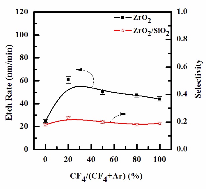
For the characterization of ZrO2 thin film in an ICP etching system, the plasma etching of ZrO2 thin film and selectivity of ZrO2 to SiO2 were systematically investigated as various etch chemistries. Figure 2 shows the etch rate of ZrO2 thin film and selectivity of ZrO2 to SiO2 as a function of reactive species concentration, when the total flow rate was maintained at 20 sccm. Other process conditions, such as RF power, DC-bias voltage, process pressure, and substrate temperature, were maintained at 600 W, - 250 V, 15 mTorr, and 45℃, respectively. Comparisons of etch rates of the ZrO2 thin film in Ar- (25 nm/min) and CF4- (44.03
nm/min) based plasmas showed that the chemical etching was more effective than physical sputtering [10]. The etch rate of ZrO2 thin film increased, while the selectivity of ZrO2 to SiO2 also increased. The maximum etch rate of ZrO2 was 60.8 nm/min at a 20% of CF4/(CF4+Ar) gas mixing ratio. It is well known that fluorine components of ZrO2 thin film form high-volatile by-product, such as ZrF4 (melting point: 450℃). The evident enhancement of the ZrO2 thin film etch rate in the pure CF4 plasmas allows one to assume that the chemical etch pathway provided by the F atom is the dominant mechanism for the given set of input process parameters [11]. In the case of the chemical etching of the ZrO2 thin films, we expect the contribution of this pathway to be much lower, compared with the ion assisted chemical reaction. The reason for this is that for ion energies of about 300 - 500 eV, typical sputtering yields for metal oxides do not exceed 0.5 - 1 atom/ion. In CF4-based plasma, addition of the CF4 up to 20% increased the etch rate through the action of two mechanisms: 1) the accelerated chemical reaction by the ion-stimulated desorption of the reaction products, and 2) increase of the contribution of the chemical etching. Nevertheless, when the CF4 content exceeds 20%, the etch rate begins to fall, due to the “disappearance” of the chemical etching [12,13].
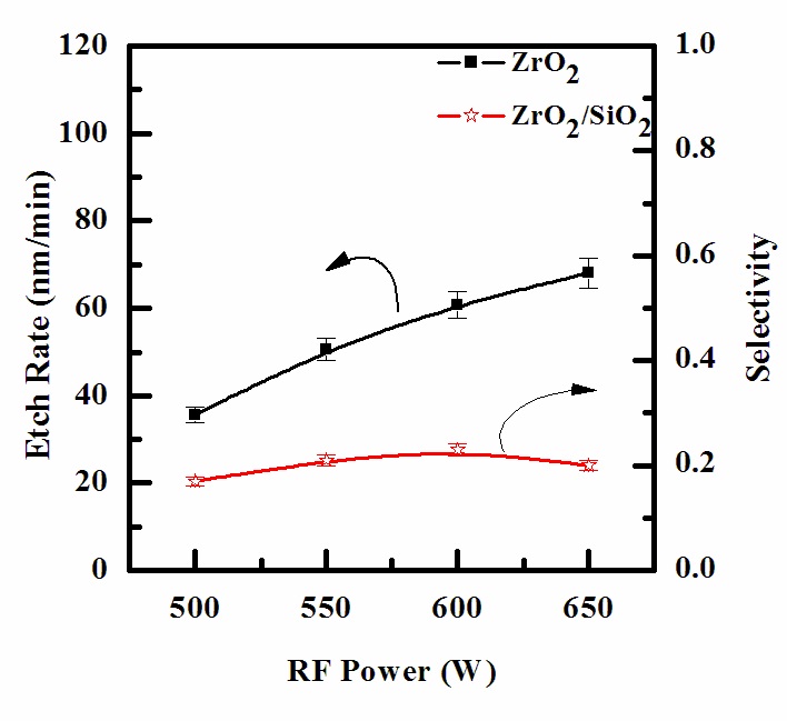
Figure 3 shows the etch rate of ZrO2 thin film as a function of RF power. Other process conditions, specifically CF4/Ar(20:80%) plasma, DC-bias voltage, and process pressure, were also maintained at - 250 V, and 15 mTorr. As RF power increases, the ZrO2 thin film also increases, starting from 35.7 nm/min at 500 W, and then reaches a maximum of 68.08 nm/min at 650 W. It can be seen that an increase in RF power causes a monotonic increase in both dissociation and ionization rates, and thus, in the densities and fluxes of F atoms and positive ions [14]. In our case, such layer can result from the deposition of solid F that is then bonded with surface oxygen to form Zr-F, as well as from F radicals incorporated in the polymer-like structure.
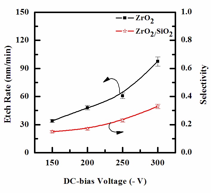
The etch rates of ZrO2 thin film are shown in Fig. 4 as functions of the DC-bias voltage. Other process conditions, namely CF4/Ar(20:80%) plasma, RF power and process pressure, were also maintained, at 600 W, and 15 mTorr. As the DC-bias voltage increases from - 150 to - 300 V, the etch rate of ZrO2 thin film increases from 33.98 to 97.5 nm/min. The selectivity of ZrO2 to SiO2 was slightly increased. An increase in etch rate can be related to the increase of mean ion energy, resulting in increasing sputtering yields for the ZrO2 thin film, and reaction products [15].
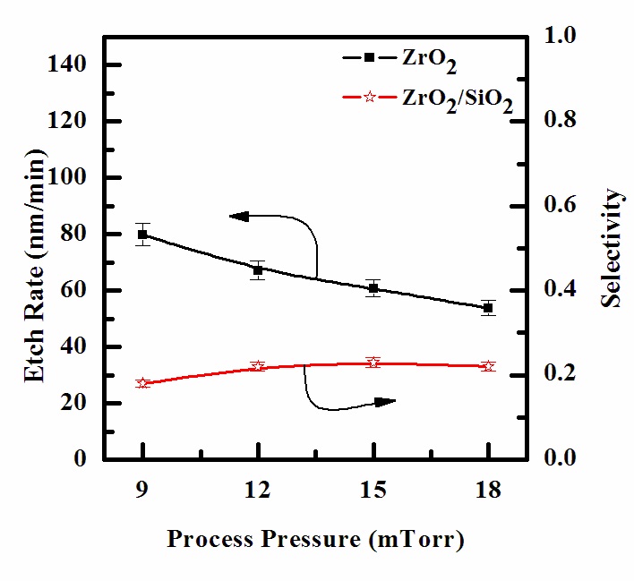
The effect of process pressure on etch rate is shown in Fig. 5.
As process pressures increased from 9 to 20 mTorr, the etch rates of ZrO2 decreased from 79.98 to 53.8 nm/min. However, we obtain a similar non-monotonic behavior, as was mentioned for the effect of the gas mixing ratio. In our opinion, the effect of gas pressure can be explained as follows: an increase in gas pressure at fixed CF4/Ar mixing ratio leads to an increase in both density and flux of fluorine atoms on the etched surface, but causes a decrease in ion flux and mean ion energy [16]. As a result, with increasing gas pressure, there is a tendency for the chemical etch pathway to accelerate, but a worse condition obtains for the ion stimulated desorption of reactive products, probably resulting in a decreasing fraction of acceptable free surface for chemical reaction [17]. Similar to the effect of the gas mixing ratio discussed above, these two factors working in opposite directions produce a non-monotonic behavior of the etch rate.
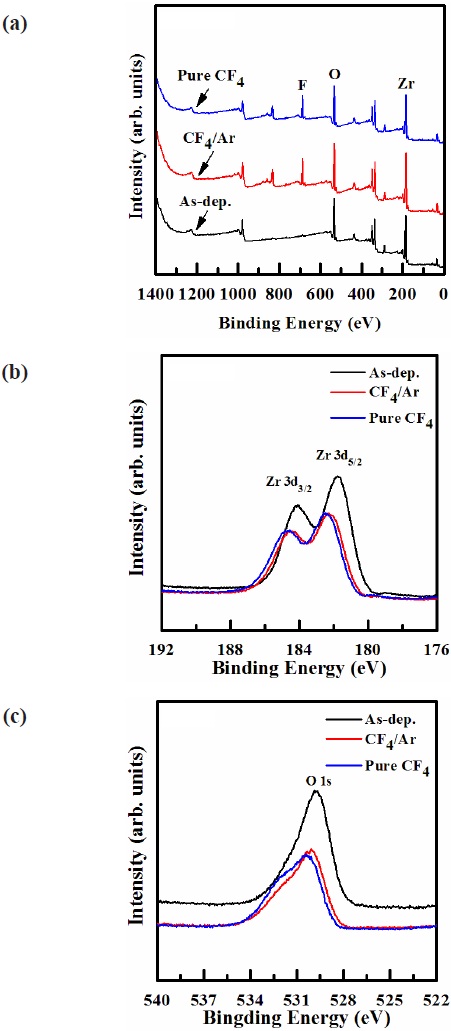
XPS analysis was performed for more detailed investigations of the chemical reaction between ZrO2 and fluorine atoms [18]. The chemical states on the etched surfaces were compared with those on the as-deposited one. Figure 6 shows the (a) wide scan spectra survey, and narrow scan spectra of (b) Zr, and (c) O, which were obtained from the ZrO2 thin film surfaces. Figure 6(b) Zr 3d photoelectron peak from the as-deposited ZrO2 thin film, which must originate from the Zr-O bonds. It can be seen that, for the as-deposited film, the Zr 3d peak can be resolved
into two peaks, viz. Zr 3d3/2 (184.1 eV) and Zr 3d5/2 (181.8 eV). For Zr 3d, it can be seen in Fig. 6(b) that when the ZrO2 thin films were exposed to both CF4/Ar (20:80%) plasma and pure CF4 plasma, the peaks of Zr 3d at 184.75, 182.45 eV, and 184.55, 182.25 eV were shifted to a higher binding energy, by about ±0.6 eV and ±0.4 eV. This chemical shift indicates that Zr chemically reacted with F, resulting in the formation of Zr-F bonds on the surface. The O 1s photoelectron peak is observed in the XPS narrow spectra of the etched ZrO2 thin film surface. As shown in Fig. 6(c), for O 1s, after etching the ZrO2 thin film in pure CF4 plasma, the shoulder peaks of O 1s decreased significantly, and the core O 1s peaks at 529.8 eV shifted to 530.5 eV, as a result of the preferential removal of Zr and O, respectively. However, when the ZrO2 thin films were etched in CF4/Ar (20:80%) and pure CF4 plasmas, the O 1s peak intensity at 529.8±0.7 eV was increased, owing to the formation of F-O bonds. The intensity of the O 1s peak for the film etched in pure CF4 plasma was higher than that of the film etched in CF4/Ar plasma, as demonstrated by the dramatic decrease in the number of F-O bonds, because of the effective dissociation of Zr-O bonds by ion bombardment. Based on the XPS result, it was revealed that Zr and O were removed by the chemical reactions with the F radicals, and by the physical bombardment of the Ar ions.
Etching characteristics of ZrO2 thin films were investigated in terms of etch rate and selectivity, using CF4/Ar plasma. Experiments were performed with variations of CF4/Ar gas mixing ratio, RF power, DC-bias voltage, and process pressure. It was found that the addition of CF4 contents up to 20% led to the etch rate of ZrO2 decreasing, in comparison with at CF4 only. The maximum etch rate of ZrO2 films was 60.8 nm/min under 20% CF4/(CF4+Ar) in 600 W, - 250 V, 15 mTorr, and 45℃. This showed that the increase of CF4 addition enhanced ion bombardment, and made the etch rate decrease. The chemical states of etched ZrO2 films were investigated using XPS, and the chemical reaction between ZrO2 and F was observed. The etching mechanism of ZrO2 thin films can be explained as follows: Zr interacted with the F radical by adding CF4, but non-volatile etch byproducts, such as ZrFx, were remained at the surface.