Oxide semiconductor-type gas sensors are more advantageous than other types of gas sensors in that not only are their sensitivity to gases high, but their response speeds are also high, and they can be easily fabricated. Furthermore, selectivity for certain gases can be generated by adding appropriate catalysts [1-7]. These sensors make use of the phenomenon that when reactant gases are exposed to the surface of the sensing materials, the electric conductivity on the surface of the oxide changes due to absorption and dissociation. To measure gas sensitivity, the temperature of the sensing materials should be maintained evenly at 300℃ or above [8]. Therefore, these sensors have a problem in that they need heaters to maintain the sensing material at a certain temperature or higher, and thus consume large amounts of power [9].
To solve the aforementioned problem, micro-sensors using complementary metal-oxide semiconductor (CMOS) or CMOSmicro- electro mechanical system (MEMS) technology have been utilized; research and development has concentrated on these micro-sensors because they have advantages such as small size, light weight, lower power consumption, high response speed, ability to be mass produced, and low manufacturing costs [10-13]. In addition, to reduce the power consumption and increase the sensitivity of gas sensors, studies on the development of nano-sized gas-sensing membranes using nano technology have been actively conducted. Since the gas-sensing characteristics of semiconductor-type gas sensors are obtained by surface reactions, gas sensors using nano materials have advantages that include low power consumption and high sensitivity [14,15]. In particular, ZnO and SnO2 are advantageous in that diverse nano structures such as nano-tubes, nano-wires, and nano-rods can be synthesized depending on the synthesizing methods and post-annealing processes.
In this study, a ZnO nanorod-based sensor and a SnO2-CuO thin film based sensor were fabricated, and then the gas sensors were exposed to carbon monoxide (CO) atmospheres of different concentrations to examine their sensing characteristics related with working temperatures. A ZnO seed layer was deposited on the platinum (Pt) micro heater using pulse laser deposition (PLD), and then ZnO nanorods were synthesized on the seed layer by hydrothermal synthesis. In addition, tin (Sn) and copper (Cu) were evaporated separately using a co-evaporation system and then thermally oxidized to form SnO2-CuO thin films.
To evaluate the CO gas-sensing characteristics of ZnO nanorods and SnO2-CuO thin films, diaphragm-type sensor platforms were generated through the following processes. To fabricate the platforms, a p-type (100) double-side polished silicon (Si) wafer with a thickness of 495 μm was used. Then, 160 nm thick low-stress nitride (Low Stress Si3N4) thin films were deposited on both sides of the silicon wafer in the low pressure chemical vapor deposition (LPCVD) method; the windows for Si anisotropic etching were formed on the back side of the Si wafer using photolithography and the reactive ion etching (RIE) method. Thereafter, for the thermal isolation of the micro-heaters to be formed on the front side of the Si wafer, the back side of the Si wafer was etched with a 30 wt% KOH solution to generate the membrane structures. Meanwhile, to make the micro-heaters and electrodes, patterns were formed using the photolithography process and Ti 20 nm and Pt 200 nm were evaporated successively using an E-beam evaporator. Then, the patterns were implemented with the lift-off method and heat treated for 30 minutes in a nitrogen atmosphere at 600℃. For insulation between the microheaters formed in this way and the sensing membranes on which electrodes would be deposited, silicon dioxide (SiO2) insulation films were deposited using the plasma-enhanced chemical vapor deposition (PECVD) method; to complete the platform, some of the SiO2 insulation films were etched using the photolithography and RIE processes.
The gas sensor platform made previously was dipped in a 6:1 buffered oxide etch (BOE) solution for 2 sec to remove natural oxide films; washed by acetone (5 min), isopropyl alcohol (5 min), and DI water (5 min) in order of precedence; and dried using nitrogen gas. On each of the washed sensor structures, a ZnO seed layer was deposited using the PLD method. Then, the platform with the ZnO seed layer was soaked in 0.1 mol, 0.2 mol, and 0.3 mol of zinc nitrate hexahydrate (Zn (NO3)2·6H2O, ZNHH;Sigma-Aldrich), hexamethylene tetramine (C6H12N4, HMT;Sigma-Aldrich) and polyethylenimine (C2H5N)n, PEI;Sigma- Aldrich) mixed aqueous solutions and heated using hot plates. The synthesis of the ZnO nanorod array was conducted at a temperature of 90℃ for 8 hours. During synthesis, temperature errors were identified using a temperature sensor and the margin of error was 90±1.5℃. When the synthesis was complete, the nanorod array was washed using methanol and DI water, in that order, and then dried for 24 hours at a temperature of 90℃. After drying, the ZnO nanorod array was heat treated for 30 minutes
in a nitrogen atmosphere at 600℃. To make the SnO2·CuO thin films, Sn and Cu were evaporated successively to thicknesses of 1000 A and 20 A, respectively, using a co-evaporation system. For the transition to heterogeneous oxide, the Sn-Cu metal layer was thermally oxidized for 8 hours in an oxygen atmosphere at 800℃ to form SnO2-CuO heterogeneous oxide thin films.
3.1 Crystal structure of ZnO nanorods and SnO2-CuO thin film
Figure 1 shows the Scanning electron microscope (SEM) images of the ZnO nanorods grown through the aforementioned processes. The ZnO nanorods grown in the 0.1 mol, 0.2 mol, and 0.3 mol precursors had an average diameter of 30 nm, 70 nm, and 200 nm, respectively. The ZnO nanorods grown in the 0.1 mol were the densest, as shown in Fig. 1. SEM images of the SnO2-CuO thin films formed through the aforementioned pro-
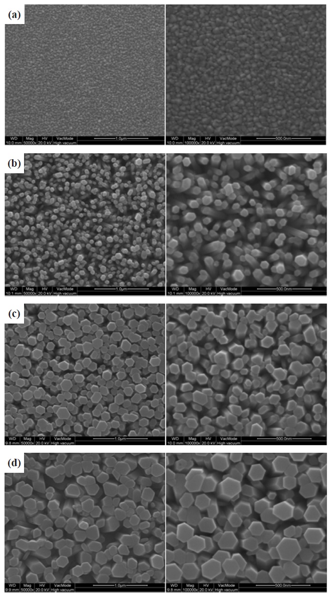
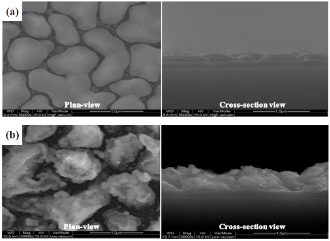
cesses are shown in Fig. 2. After annealing at high temperatures, the surface area in which gas can be adsorbed was increased, as shown in Fig. 2.
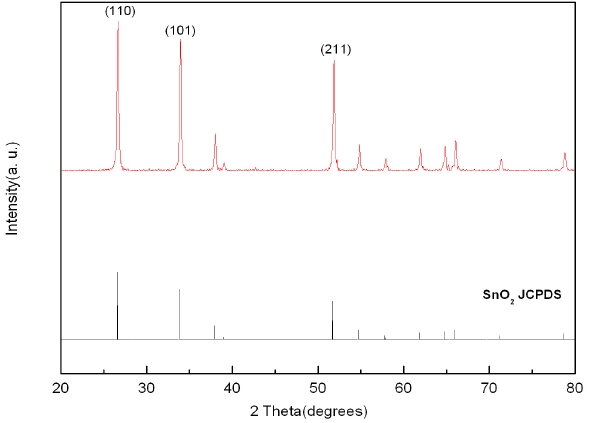
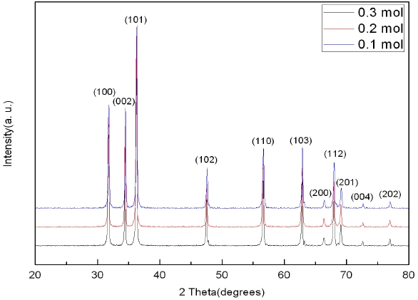
Figure 3 shows the results of X-ray diffraction analysis of ZnO nanorods grown using the hydrothermal method. Impurities other than ZnO are observed. Various peaks related to ZnO were observed in all cases due to the irregularity of growth directions. It can be seen that there are some differences only in the intensity of peaks in all cases. Figure 4 shows the results of X-ray diffraction curves of SnO2-CuO thin films. Only the dominant peaks of (110), (101), and (211)-oriented SnO2 were observed, but the CuO peaks were not observed. This is because the Cu layers deposited on Sn were very thin and thus crystalline structures could not be formed. It was identified that the SnO2-CuO thin films analyzed based on X-ray diffraction were almost the same as the joint committee on powder diffraction standards (JCPDS) of SnO2.
3.2 Sensing characteristics in relation to working temperatures
The CO gas-sensing characteristics of the ZnO nanorod and SnO2-CuO thin film gas sensors were evaluated under a CO gas concentration of 10 ppm at temperatures ranging from 150℃ to 400℃ at a difference of 50℃, and the results were compared with one another. The sensitivity was identified as the ratios of
the difference between the sensor resistance in the air (Ra) and the sensor resistance during the gas reactions (Rg), as shown in expression (1):
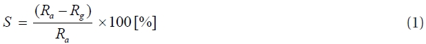
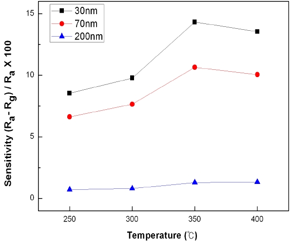
Figure 5 shows the sensitivities of the ZnO nanorod sensors with an average diameter of 30 nm, 70 nm or 200 nm under 10 ppm of CO gas at different working temperatures. It can be seen that the overall tendency shows higher sensitivity values, as working temperatures increase to show the highest sensitivity values when the working temperature is around 350℃. When oxygen ions are absorbed on the surfaces of ZnO nanorods, they are absorbed in the form of O- ions at 300℃ and in the form of O2- ions at 350℃. Each of the absorbed O- ions reacts with CO gas as shown in expression (2) to discharge one electron:


On the other hand, each of the O2- ions reacts with CO gas as shown in expression (3) to discharge two electrons thereby enhancing the conductivity, and thus the sensitivity at 350℃ is shown to be higher than the sensitivity at lower temperatures. However, in the case of 400℃, although oxygen ions are absorbed on the surfaces of ZnO nanorods, due to excessively high temperatures, some of the O2- ions that react with CO gas are detached due to the thermal energy and thus the sensitivity decreases. The smaller the average diameter of the nanorods, the higher the overall sensitivity became. In the case of nanorods with an average diameter of 30 or 70 nm, as working temperatures increased, the sensitivity also increased. However, in the case of nanorods with an average diameter of 200 nm, no large difference could be observed.
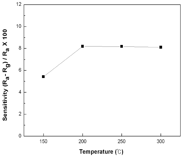
Figure 6 shows the sensitivities of the SnO2-CuO sensors under 10 ppm of CO gas at different working temperatures. The overall tendency was that although the sensitivity increased as the working temperature increased, it was shown to be almost the same at temperatures exceeding 200℃. This phenomenon can be explained through the results of a study by Yamazoe [15]. As the temperature increased, the speed of CO molecules to be absorbed by or detached from the surface of SnO2 increased until it arrived at its highest value at a certain temperature. The temperature with the highest sensitivity and optimum reaction speed would be determined by the speed of absorption and detachment of gas molecules to the surface of the sensor. The highest sensitivities were 8.19 % and 8.18 % at 200℃ and 250℃, respectively.
3.3 Sensing characteristics in relation to gas concentrations
To measure the sensing characteristics of the ZnO nanorod sensors in relation to CO gas concentrations, the sensitivities were measured at a working temperature of 350℃ at different CO concentrations. Figure 7 shows the sensing characteristics of the ZnO nanorod sensors with an average diameter of 30, 70, or 200 nm when the carbon monoxide (CO) gas concentration was 1 ppm, 10 ppm, or 100 ppm. The overall tendency was that the sensitivity increased as the gas concentration increased, although the sensitivities were shown to be almost the same when the average diameter of the ZnO nanorod sensors were 200 nm. The ZnO nanorod array with the average diameter of 30 nm had
a sensitivity that was 1.5 times and 13 times higher sensitivity than the 70 nm and 200 nm nanorod arrays, respectively. The reason for these results is considered to be that nanorods with smaller diameters have wider surface areas.
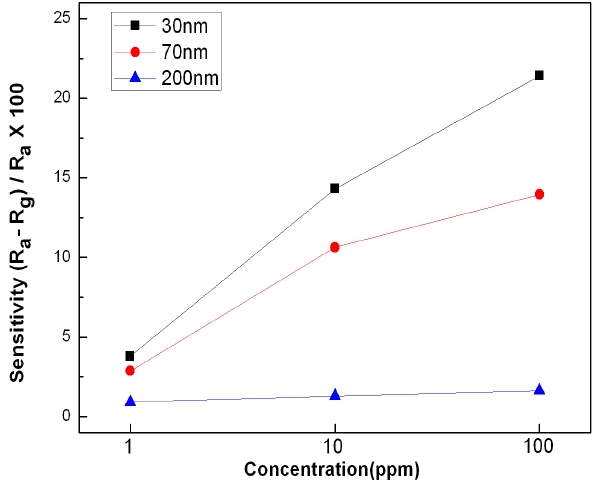
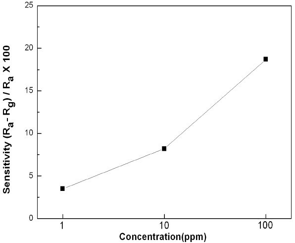
Figure 8 shows a graph of the relationship between the sensing characteristics of SnO2-CuO sensors at a working temperature of 200℃ with CO gas concentrations of 1 ppm, 10 ppm, and 100 ppm. The overall tendency was that as the concentration increased, the sensitivity increased. The sensitivity measured at a concentration of 100 ppm was about 2.3 times higher than the sensitivity measured at a concentration of 10 ppm. At a concentration of 1 ppm, the sensitivity was 3.5 %.
In this study, MEMS gas sensors were made using ZnO nanorod arrays and SnO2-CuO heterogeneous oxide thin films. The sensing characteristics for CO gas were evaluated, and the conclusions obtained through the evaluation are as follows. Gas sensor platform-embedded micro heaters and sensing electrodes were fabricated on Si substrates using the conventional MEMS process. The ZnO nanorods were grown on a ZnO seed layer using the hydrothermal method by changing the concentrations of its precursors (ZNHH, HMT, PEI). The average diameters and lengths of the grown ZnO nanorods were 30~200 nm and 150~300 nm, respectively. These sensors showed a sensitivity of 1~21% under a CO concentration of 1~100 ppm at a working temperature of 350℃. In addition, highly pure Sn and Cu metals were evaporated on the sensor platform. Next, the metals were thermally oxidized for 8 hours in an oxygen atmosphere at 800℃ to form SnO2-CuO heterogeneous oxide thin films. These sensors showed a sensitivity of 3~18% under a CO concentration of 1~100 ppm at a working temperature of 200℃.