In the flat panel display industry, the OLED (organic light emitting diode) based display is expanding rapidly. It has been mainly used as a small size display for mobile phones. Recently, the OLED based display is taking aim at the flat TV market. Display by thin OLED panels has wider view angle and better flexibility compared to those of LCDs. Among several OLED panel fabrication methods, the fine metal mask (FMM) method has most often been used for fabrication of displays. Fine patterns of pixels made on a metal mask let thermally evaporated molecules pass through. In the FMM method, mechanical support and alignment of the thin and fine metal mask imposes technical difficulties at a scale large enough for TV panel fabrication. The inkjet method is rapidly developing and it should become another competitive method for large area OLED panel fabrication. However, mixing of different ink during the process of multi-layer stacking, inaccurate control of ejected ink, and poor pixel resolution are still problems.
There are several laser methods for OLED fabrication, and among these, laser thermal printing [1-6] and laser sublimation [7,8] are the main methods. A laser thermal printing method, which was originally developed for fabrication of the color filters for the LCD panel, was suggested as an alternative method of OLED fabrication [9]. In view of mass productivity, high resolution, multi-layer stacking, and scalability to large size mother glass, the laser method has potential for competing technology [1,3]. In previous studies of the laser thermal printing method, dithering of a laser beam was used for OLED panel fabrication [1, 3, 4]. J. Kwon et al. suggested sine, saw tooth, and trapezoidal waveforms for clean patterning because a Gaussian waveform has highest energy at the center of the beam [3]. However, the effects of dithering waveforms on the printed patterns and analysis of donor film after transfer have not been investigated yet.
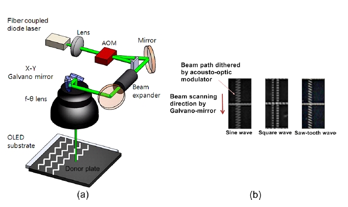
A compact laser thermal printing device which employs a single mode cw (continuous wave) fiber laser was fabricated for analysis of the dithering beam effect on printed patterns. Small volume, short turn on time, and alignment free characteristics of the fiber laser should be advantageous when mass production is considered. The fiber laser beam was dithered by an acousto-optic modulator (AOM). Three different functional waveforms, sine wave, square wave, and saw tooth wave, were tested for dithering. The profiles of organic film on the donor plate as well as on the OLED substrates were investigated after the printing. Also, the performances of OLEDs printed by three different kinds of dithering laser beam were compared.
A fabricated laser thermal printing device consists of a printing laser, beam expanding and delivery optics, and a mechanical part. The optical and mechanical structures of the device are shown in Fig. 1 [10]. A linearly polarized, Gaussian-like LP01 spatial mode beam from a cw fiber laser (IPG Photonics) was collimated by a lens set. The maximum power of the fiber laser was 10 W and the wavelength was 1060~1070 nm. The collimated beam was transmitted through an acousto-optic modulator (AOM). The laser beam diameter after the AOM (AA Opto-Electronic) became enlarged by being transmitted through a variable beam expander (LINOS, 2×~8×). The expanded beam was sent to a Galvano-mirror pair (SCANLAB). The laser beam reflected by the Galvano-mirror was focused by an
maximum scan area of the focused laser beam was 100×100 mm2. The beam size at focus depended on the expansion ratio of the beam expander, and the minimal spot size of the focused beam, which limited the spatial resolution in the printed pattern, was 30 μm. The beam size at focus,
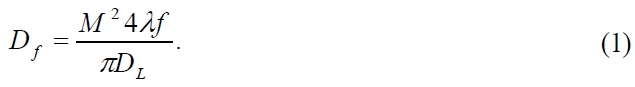
where
The donor plate and OLED substrate were firmly held on a flat stage where small holes were made for air suction, and an oil-free diaphragm vacuum pump was connected to the mounting stage. To remove moisture and oxygen in the air, which degrade efficiency of the OLED considerably, the mounting stage was installed inside a vacuum chamber. The chamber was evacuated of air (~20 Torr) by the same vacuum pump and was filled with dry nitrogen gas. The process was repeated two times to remove oxygen and humidity before the laser printing experiment. Overall the laser thermal printing device had compact dimension of 0.8 ×0.8×1.5 m3, including laser, pump, personal computer, metal box containing optical parts, vacuum chamber, and related driving electronics [11].
The propagation direction of the laser beam was deflected while passing through an AOM due to diffraction by periodic refractive index variation in the AOM. Maximum deflection angle of the diffracted beam in first order was 49 mrad when the RF frequency fed to the AOM was 125 MHz. At this RF frequency, about 70% of the fiber laser beam was deflected by the AOM in the first order diffraction. The RF frequency applied to the AOM was variable from 95 MHz to 125 MHz as a linear function of a modulation signal of 0~5 V from the function generator. The deflection angle of the laser beam was modulated in the range of 37 mrad to 49 mrad as a linear function of the RF frequency. Three periodic waveforms; sine, square, and saw-tooth waves from function generator, were tested as modulation signals. In the experiment, the frequency of modulation signal was pre-selected in the range of 100 Hz ~10 kHz and the linearly scanning laser beam by Galvano-mirror was dithered following the pre-selected frequency. The frequency of the modulation signal was selected considering the scan speed of the beam and the laser power. The scan speed was decided by the rotation speed of Galvano-mirrors and focal length of the
Figure 1(b) shows typical traces of laser beam recorded on a photographic paper when sine wave, square wave, and saw tooth waves were applied to the acousto-optic modulator. The laser beam was dithered at 1 kHz in the transverse direction to the beam scanning direction guided by Galvano-mirror. The scan speed of the focused beam at the paper was 500 mm/s. Although beam paths became broader due to burning of the photographic paper by the laser beam tail, each beam path showed a different trajectory depending on the waveform of modulation signal applied to the AOM.
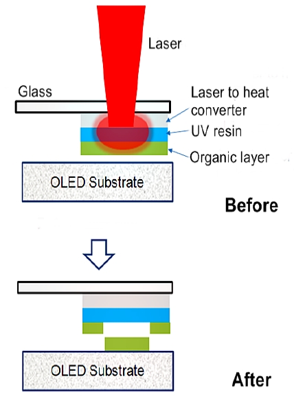
Instead of a polymer sheet [12,13], a glass plate with 0.7 mm thickness was used as a substrate for a donor plate. Figure 2 shows the schematic structure of the fabricated donor plate. A laser-to-heat converting (LHC) layer was made by a spin coating a mixture of carbon black (Tokyo Ohka Kogyo, BK-3110SL) and UV (ultra-violet) resin (Kolon, CS-320E3) with a thickness of 800 nm on the glass plate surface. We also tried silk printing; however, the surface flatness was much better when the spin coater was used. After the UV curing LHC layer, the surface of the layer was spin-coated by another UV resin (KOLON, CS-320E3) with thickness of 1.5 μm to form a release layer. The UV cured release layer prevents penetration of carbon black particles contained in the LHC layer to the organic material film.
The flatness of the each layer on the donor plate affected the laser thermal printing quality considerably. Small craters or digs on the surface due to dried micro-bubbles were the main faults in the donor plate. The Alq3 film was coated on the release layer by thermal evaporation. The Alq3 film coated donor plate was in contact with the OLED substrate as shown in Fig. 2. When the focused laser beam irradiated the LHC layer, the carbon black of the LHC absorbed the laser light, and the light energy was converted into thermal energy. The generated heat expanded the LHC layer as well as the release layer. Expansion of the donor surface
was detected by monitoring the temporal profile of the reflected He-Ne laser beam on the surface. The expansion weakened the adhesive strength between the release layer and the Alq3 film. The coated Alq3 film was peeled off and printed on an OLED substrate with help of the pressure exerted by the expanding LHC layer.
The transfer of organic film, coated on donor plate, to the OLED substrate was observed when the laser power exceeded a threshold power density. At very high laser power, not only the organic film but also the release layer was peeled off from the LHC layer. Once the release layer was detached from the LHC layer, the donor plate surface deformed from flat shape to curved wrinkles resulting in an irregularly printed profile. To find the optimal condition which gave detachment of organic film only, we repeated several trials while adjusting the laser power. The results in Fig. 3~ Fig. 7 were obtained by sending laser power of 0.26 W for a sine wave, 0.27 W for a square wave, and 0.22 W for a saw tooth wave to the donor plate. Optimal laser power was decided by measuring brightness of fabricated OLEDs as a function of applied current. The scan speed of the focused beam in the donor plate was slowed down to 50 mm/s and the dithering frequency was set at 1 kHz in the printing.
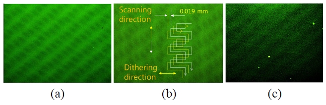
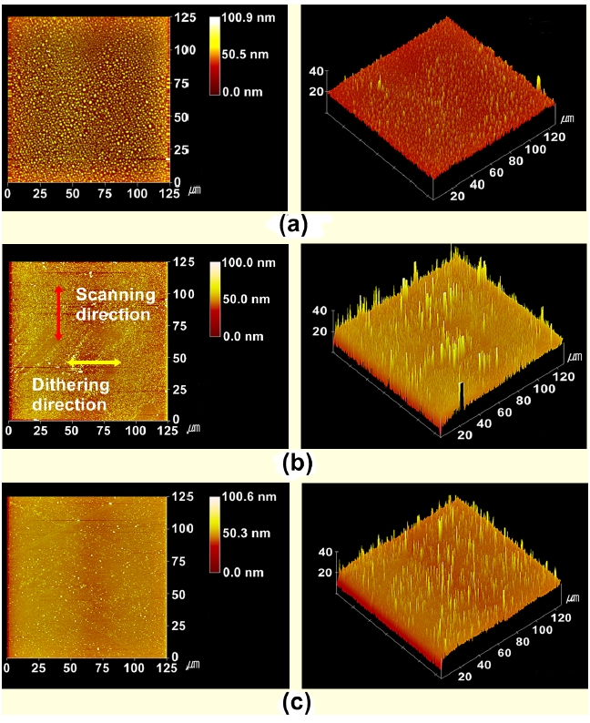
The fluorescence microscope images of Alq3 on the donor plate after the laser printing process are shown are shown in Fig. 3 for three different dithering waveforms. Dark-dotlike parts are displayed in a regular pattern. The thickness of Alq3 film at these dark areas of pattern is thinner than that of bright areas of the plate. It means that Alq3 film in the bright green area is less transferred to the OLED substrate. The zigzag lines in Fig. 3(b) shows the paths of focused laser beam patterns and the arrows indicate directions. In the printing, the pitch (distance between the parallel lines that the Galvano-scanned laser beam makes) was preset at 0.019 mm in the Galvano-mirror control program. Then the program controls the Galvano-mirror to fill in a square box by drawing parallel lines as indicated in Fig. 3(b). The zigzag lines were generated by dithering, and the half width of the dithered beam was about 0.06 mm for modulation amplitude of 1 V. With the offset voltage of the function generator set at 1V, the modulation signal varies between 0 V to 2V. At this voltage changes, the beam dithering angle change by the AOM was 4.8 mrad. After the beam expander, the angle was reduced to 1/6 of the
original one. The dithering beam width was close to the estimation calculated by using
The pattern of Alq3 after dithering by square wave (Figure 3(b)) was very different from the case when sine wave was applied (Figure 3(a)) although laser power, scan speed, and modulation frequency were the same. The dark spots became elongated in the scanning direction. Figure 3(c) shows the result when the saw-tooth wave was sent to the AOM. The dark spot was blurred and the scanned area became brighter than for the other cases over the printed surface. The printed pattern of the saw-tooth wave case showed the most improved uniformity compared with those of the other cases.
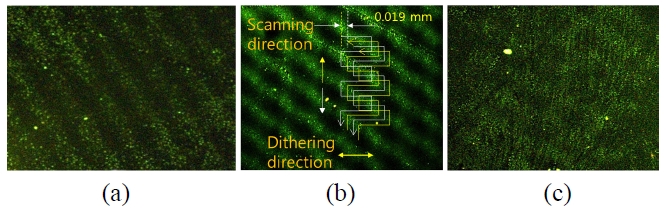
The profiles of Alq3 film attached to OLED substrates corresponding to each case of donor plate shown Fig. 3, were examined by fluorescence microscope images of the corresponding pattern of printed Alq3. Figure 4(a), (b), and (c) corresponds to the cases when sine wave, square wave, and saw tooth waves, respectively, were applied to the AOM. The printed images and beam traces are mirror images of those in Fig. 3. By comparing the images, we can see that the Alq3 film detached from the donor plate is attached onto the OLED substrate. However, the shapes of bright patterns of OLED substrate do not match exactly with dark patterns of donor plate. The patterns on the OLED substrate are blurred compared with those of the donor plate. Among the printed patterns, the case where the saw tooth wave was applied is most uniform. However, the images of Alq3 attached on OLED substrate are most clearly observed for square wave and sine wave cases. The results show that uniformity and the amount of transferred organic film strongly depend on the dithering beam trajectories.
To investigate the profile of detached material in detail, we took AFM (atomic force microscope) images of donor
plates after laser printing. These profiles were used to obtain results in Fig. 3. Figure 5(a) shows the result when sine wave was applied to the AOM. The detached profile of the Alq3 film from the donor plate shows crests and troughs clearly. Very fine wrinkles in Figures 5(a)~5(c) were observed when we applied Ar plasma for 90 seconds on the Alq3 coated surface before laser printing. The surface treatment using plasma was an attempt to transfer Alq3 only, without affecting the release layer. For the case of the square wave shown in Fig. 5(b), the dark area was slightly elongated along the scanning direction compared with that of the sine wave case. But, printed patterns of both cases are more clear than those of the saw-tooth wave case, implying thicker coated film. Judging from detached film profiles measured by AFM, the saw tooth wave gave the most uniform profile and the sine wave transferred the largest amount of film. The result was expected from the recorded trajectory shown in Fig. 1(b) where the line at both edges of the dithered pattern were wider for the sine wave and the square wave cases than for the saw tooth wave case. As scan speed of the beam at turning points of the trajectories for both cases are slower than for the saw tooth wave case, more Alq3 film was transferred. Although we tried to smooth out the nonuniform distribution of incident energy caused by different scan speeds of beam by repeated scans with minimal allowed pitch, it was not enough. As can be seen in Fig. 3 and Fig. 4, the phase shift between adjacent dithering beams makes part of the beam trajectories overlap. The
overlapping beam trajectories make wide oblique traces of transferred film. As the horizontal speed of the dithered beam was much faster than the vertical speed of Galvanoscanning, more organic film on the vertical line was transferred to the OLED substrate. This indicates that uniformity of total irradiated laser energy (power × irradiation time) is crucial for uniform transfer of organic film. The uniformity can be enhanced through fine adjustment of relative phase between the dithering beam belonging adjacent lines. Finding suitable dithering waveforms other than conventional waveforms used in this experiment is also demanded.
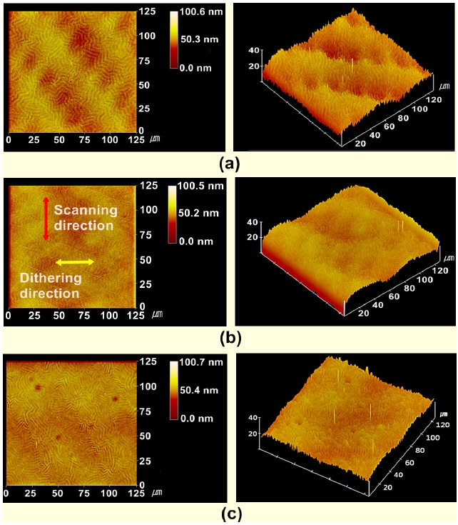
Figure 6(a), (b), and (c) show the AFM images of organic film coated on the OLED substrate by laser thermal printing. The AFM images are also different from negative
images of the donor plate, similar to the results of the fluorescence microscope image. The patterns are blurred, implying that part of the Alq3 film was detached from the donor plate in the vapor phase by sublimation, and expanded vapor attached onto the cold OLED substrate [14]. For detailed analysis, calculation of total laser energy per unit area, temperature as a function of space and time, and vapor rate on temperature distribution are needed [15].
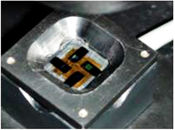
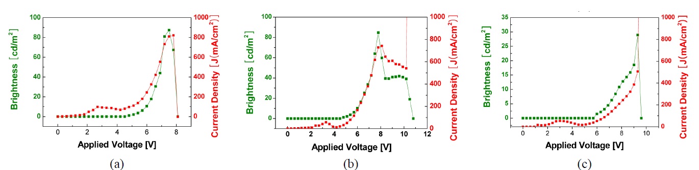
The process of OLED fabrication and device performance tests were the same as before [10]. Sine, square, and saw tooth waves were applied to the acousto-optic modulator. After the organic material printing, Al electrode was deposited on the surface by thermal evaporation. The fabricated OLED was installed inside a testing mount as shown in Fig. 7. When the donor plate surface was rough and had digs, fabricated OLEDs showed dim emission or no emission. After several trials, we could find conditions for stable emission. Typical results of measured brightness and current density of OLEDs as a function of applied voltage are shown in Fig. 8. Contamination due to humidity and oxygen while transporting the laser printed OLED substrate to the metal coating chamber made the performance worse. The fabricated OLEDs using the dithering beam by square wave or sine wave showed similar results. They showed brighter emission at low voltage compared with that of the saw
tooth wave case. Although both sine wave and square wave gave better OLED performances, the surface uniformity was better for the saw tooth wave case. AFM and fluorescence images indicated that the amount of transferred film was larger for square wave and sine wave cases, and the larger amount produced better performance.
The dependences of detached Alq3 film profiles on dithering waveforms in laser thermal printing were analyzed by fluorescence microscopy as well as AFM (atomic force microscopy). Three different waveforms, sine, square, and saw tooth, were tested. For each case, the profiles of removed organic film were different from that of printed film as partial sublimation of Alq3 film blurred the pattern. To see the effects of the dithering waveform on current-to-emission performances of OLEDs, we applied each dithering waveform to print Alq3 film. The electricity-to-light conversion performance was better when a square wave or sine wave was used because more organic film was transferred compared with the case of a saw tooth wave. Although we tried partial overlapping of adjacent scanning laser beam trajectories on donor plate for more uniform printing, it made oblique thick traces of densely overlapped trajectories due to phase lag between adjacent dithering beams. The result demonstrated that precise control of relative phase of adjacent dithering beam or design of better modulation waveform, other than the conventional waveforms used in this experiment, was required for uniform printing of organic film. In this view, beam specially shaped by optical methods, instead of a dithering laser beam, can be another candidate for uniform printing methods [16].