A microcolumn is a miniaturized low-energy electron beam column proposed by Chang et al [1]. It has the length of one hundredth of a conventional electron column at comparable efficiency and therefore can be setup in an array of multiple columns working in parallel [2]. The microcolumn has many advantages; it can reduce the device damage due to lower voltage operation. It is also possible to irradiate insulating devices without significant surface charging because of the considerably reduced electron penetration into the test samples [3]. Microcolumns have attracted much attention for a variety of applications, such as miniaturized scanning electron microscopes (SEM), electron beam inspection, metrology, electrical testing, and electron-beam lithography [4-5].
As an inspection application, microcolumns have demon-strated the possibility of inspecting open defects in a display panel thin film transistor-liquid crystal display (TFT-LCD)[6-7]The raster scan images of TFT-LCD panel were obtained using a 300 eV micro-column under specific operation conditions. The results showed that a low energy microcolumn can be adopted in the production process to detect the location and types of various open defects. For large panel inspection, an electron column must have a large scan field without astigmatism and distortion for the panel product.
For such large sample inspection applications, we proposed an advanced micro-column to achieve a low-aberration and low-distortion electron beam while maintaining the wide deflection field [8]. The newly designed microcolumn has column structure similar to the conventional one except that the einzel lens consisted of four electrodes. The central electrode of the conventional einzel lens was replaced by two electrodes with keyhole-shaped apertures. Additionally, the arrangement of the double deflector and einzel lens was changed. The electron optics of the deflector and the focusing lens of the new microcolumn were analyzed and optimized as described in the previous paper [8]. The analysis results showed that an advanced microcolumn with EQ-einzel lens provides a high-resolution beam uniformly and with lower distortion over the whole deflection field. It indicates that the beam spot became smaller than in the double deflectors of the conventional microcolumn.
In this paper, we report the construction and operation of the newly designed microcolumn with keyhole-shaped apertures. The preliminary results of this advanced micro-column will be presented.
2.1 EQ-Einzel Lens Design & Construction
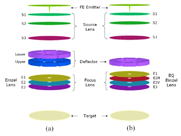
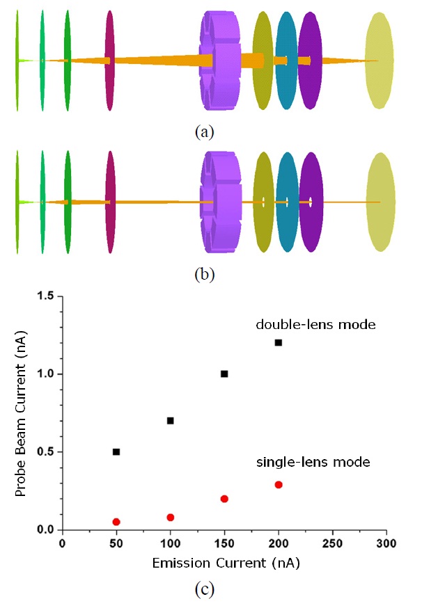
A conventional microcolumn consists of a cold field emitter, a source lens for extracting, accelerating, and controlling an electron beam, an einzel lens for focusing the electron beam, and double deflectors for deflecting the electron beam onto a specimen target. Typically double deflectors,which consist of a lower and upper deflectors, are located between the source lens and the einzel lens. Einzel lenses have three electrode pairs, each with a circular aperture, as shown in Figure 1(a). However, in this study, a newly designed microcolumn has a single deflector and an einzel lens having four electrodes as shown in Figure 1(b). The two central electrodes having keyhole-shaped apertures in the new einzel lens were defined as an electrostatic quadrupole lens (EQL). The reason that we did not attach an aligner that corresponds to the lower deflector is because we wanted to only test the performance of EQL. The design of the deflection system is expected to change in the future.
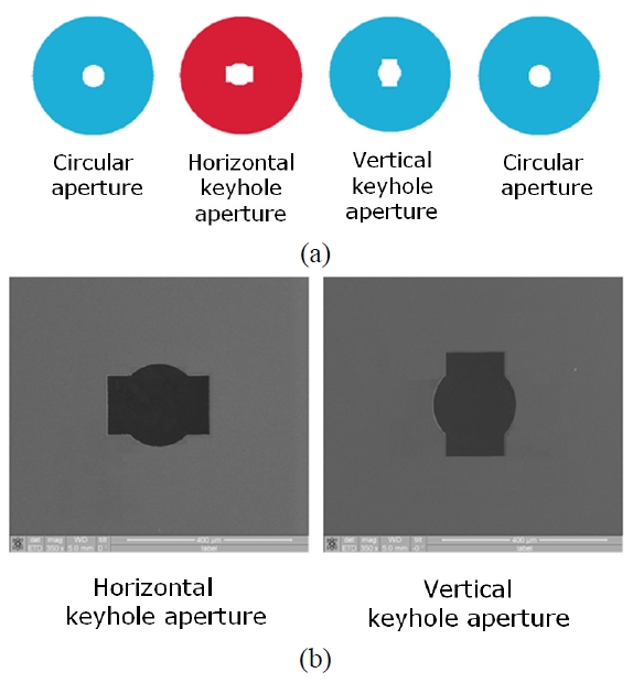
Figure 2(a) shows components of the EQ-einzel lens composed of two circular aperture and two keyhole-shaped apertures perpendicular to each other. The circular aperture components were constructed using MEMS technology on about 3 ㎛ thin Si membrane. The details of construction of such circular einzel lens components can be found elsewhere [9]. The keyhole-shaped apertures are made by overlapping a rectangular aperture of 150 ㎛ × 250 ㎛ on a circular aperture of 200 ㎛-diameter as showing in Figure 2(b). In this study we created the circular aperture on the Si membrane by MEMS process first, and cut the rectangular-shape over the circular aperture to form a keyhole-shaped aperture using a focused ion beam (FIB) systems. However, full construction to make the keyhole-shaped apertures can be done by the MEMS process.
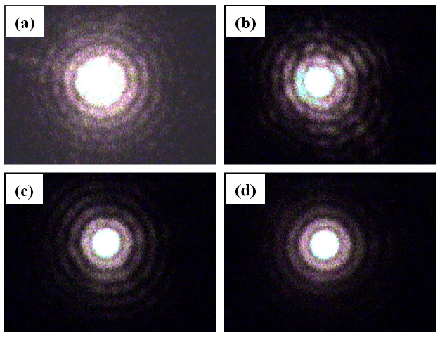
The two keyhole-shaped apertures are located in between two circular apertures. The EQL is constructed by using two opposing plates with elongated rectangular apertures in 90 degree staggered positions, and different potentials are applied to each electrode. The alignment of the EQ-einzel lens is an important factor for microcolumn operation. The spacing between two electrodes ranges from 150 ㎛ to 500 ㎛. The alignment between lens apertures was performed using laser diffraction patterns, such as an Airy-type circular diffraction pattern, through circular apertures [10-11].
Figure 3(a) to (d) show Airy-type circular diffraction patterns using the laser diffraction patterning method. Laser beams passing through the apertures of the micro-lenses form diffraction patterns. Figure 3(a) is the diffraction pattern of the first circular aperture. Figure 3(b) is the diffraction pattern image according to the alignment status of the second electrode which is a keyhole shape, in front of which the first circular aperture is located, when the centers of the two apertures are aligned exactly in the optical axis. Figures 3(c) and 3(d) are diffraction pattern images of three and four assembled apertures, respectively. The laser pattern method produced fairly good results for the alignment of the four apertures. In general, the pattern showed perfect rings where the intensity distribution was also bearing circular symmetry. If one aperture moved perpendicular to the optical axis, then the circularity was reduced and the intensity distribution lost its symmetry. This occurred between the first and second apertures.However, the alignment error of four apertures was measured to be less than 13 ㎛ across the optical axis using an optical microscope[11].
2.3 Operation of EQ-Einzel Lens
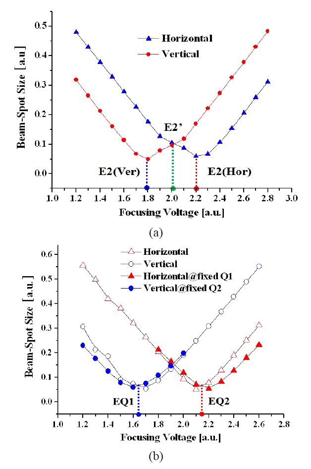
Figure 4 shows the adjustments of focusing voltage at a conventional einzel lens and an EQ-einzel lens.
A conventional einzel lens has three electrodes for focusing a beam. Typically the grounded voltage is applied to the outer two electrodes and the focusing voltage to the central electrode. A voltage difference occurs due to the astigmatism between horizontal [E2(Hor)] and vertical [E2(Ver)] focusing as shown in Fig. 4 (a). The horizontal and vertical directions are defined the same as in the keyhole-shaped apertures as shown in Fig. 2. Thus, the focusing voltage [E2] is determined by considering both directions. On the other hand, the EQ-einzel lens provides an adjusting function of astigmatism when a different voltage is applied to the two opposing electrodes. Thus, each direction of vertical [EQ1] and horizontal [EQ2] keyhole electrodes are applied independent voltages as shown in Fig. 4(b). As a result, EQ-einzel lens can achieve a high-resolution beam uniformly and lower distortion over the deflection field.
The advanced microcolumn with EQ-einzel lens has been tested in two types of operation modes. Typically, the microcolumn is operated in single-lens mode and its optical properties have been analyzed in detail [12]. In this mode, the e-beam extracted from a field emitter made out of tungsten wire by using an electrochemical etching method, is focused into a Gaussian spot using an electrostatic einzel lens, and the focused beam is scanned across the substrate
with an electrostatic deflection system. A limitation of the microcolumn operating as a single-lens system is its lack of flexibility in simultaneously providing the desired high beam current at small spot sizes, because a small amount of the electrons extracted from the field emitter can pass through a limiting aperture when a tip voltage is determined. To solve the single-lens problem, we replaced the simple gun extraction optics with an electrostatic condenser lens in the microcolumn operation to achieve double-lens configuration [13]. Thus the amount of emission current passing the limiting aperture can be controlled by the source lens.
Figure 5 (a) and (b) show simple optics diagrams of single-lens mode and double-lens mode operations of the microcolumn. Figure 5(c) shows measurement results of probe beam currents at two operation modes when the emission current of field emitter range from 50 nA to 200 nA. At the emission current of 50 nA, a probe beam current at double-lens mode was measured ~ 0.5 nA at the sample. This current value was ten times higher than that of ~ 50 pA at single-mode operation. In general, we can obtain very high probe beam current.
We evaluated the EQ-einzel lens microcolumn in single-lens mode and double-lens mode. The column configuration is
similar to a conventional microcolumn except for the einzel lens structure. A working distance between the last electrode of the einzel lens and the sample is about 3.8 mm. A test sample of a 400 mesh Cu-grid is attached.
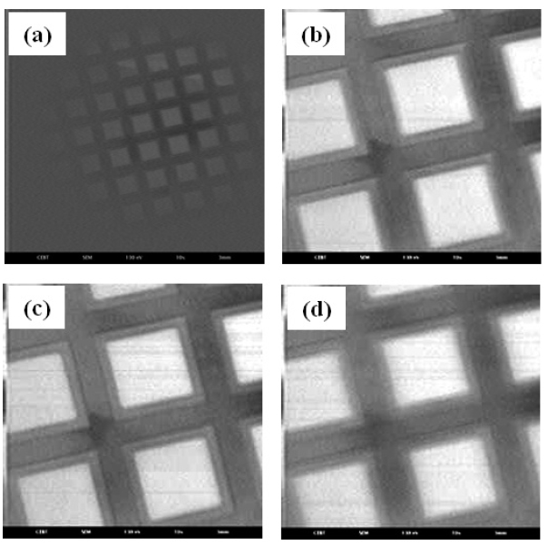
The preliminary results of the EQ-einzel lens effects at these two mode operations are shown in Figure 6 and Figure 7. For the single-lens mode, a negative voltage was applied to the electron emitter, and the electrostatic source lenses (an extractor [S1], an accelerator [S2], and a limiting aperture [S3]) are usually grounded. The einzel lens was used to focus the electron beam by applying a retarding or an accelerating voltage to the center electrode [E2] of the einzel lens, with the first [E1] and third [E3] electrodes being grounded. Therefore, the energy of the electron beam arriving at the sample depends only on the potential applied to the electron emitter's tip.
A negative voltage of -300V was applied to the emitter, and extraction emission of 50 nA was set by applying adjustable voltage to extractor electrode (S1). The identical voltage was applied to two outer electrodes and the focusing voltage to the two inner electrodes. Figure 6(a) is a single-lens mode image when a focusing voltage of 502 V was applied to the second horizontal keyhole aperture electrode [E2H] and third vertical keyhole aperture electrode
[E2V] of the EQ-einzel lens, and first [E1] and fourth [E3] electrodes were grounded. The adjustments of focusing voltage and deflection scan view in the EQL are showing in Figure 6(b) to (d). At a condition of the voltages of E2H = 508 V, and E2V = 502 V, the quadrupole lens provided a well-focused image over full scan area of 140 ㎛ × 140㎛ as shown in Fig. 6(c).
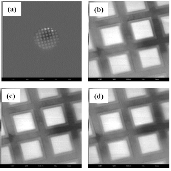
For the double-lens operation, a negative voltage was applied to an accelerator electrode [S2], and the e-beam was slightly diverged and converged to make a crossover between S3 and the einzel lens. After that, additional focusing voltage was applied to the einzel lens to be focused at the substrate plane. Thus both source lens and einzel lens acted as focusing lenses.
In this experiment, the tip voltage of -300 V and emission current of 50 nA were applied to the micro-column. A negative voltage of -243 V was applied to S2 electrode, and all einzel lens electrodes were grounded to obtain focusing image by the first lens as shown in Figure 7(a). The sample image was blocked by the einzel lens, because a scan-deflector was located between the source lens and the einzel lens. After that, the image was defocused by applied voltage of -225 V to converge the beam. Finally, additional voltages of E2H and E2V were applied to form a focusing image by double-lens mode as shown in Figures 7 (b) to (d). The results show that the EQ-einzel lens provided a good focusing image without astigmatism when we applied the different voltage of 456 V at the horizontal keyhole electrode and 450 V at the vertical keyhole electrode as shown in Fig. 7(c). In general, the results show that the double-lens mode has higher probe beam current, and can obtain larger distortion-free images compared with the single-lens mode.
We proposed, created, and demonstrated an advanced microcolumn design with an EQ-einzel lens for large scan field applications. The design is as simple as a conventional microcolumn. We can also utilize the same fabrication process for the EQ-einzel lens. The advanced microcolumn with the EQL was tested in single-lens mode and double-lens mode. The preliminary results show that the EQ-einzel lens provided an adjusting function of the astigmatism when different voltages were applied to the two inner electrodes. It also shows that the ELQ compensates the deformation of the beam-spot shape over the whole deflection field. The EQ-einzel lens microcolumn can be applied to large-scale sample inspection applications.