Plastic optical fiber (POF) is widely used and widely regarded in short-reach network systems, such as automotive network, office network, home network, audio interface, and IEEE1394. POF can be easily aligned and quickly installed due to its large diameter compared with a glass optical fiber. Recent advances in poly methyl metacrylate (PMMA) POF allows it become a powerful alternative to copper cables in short-reach applications. High-speed networks such as media oriented systems transport (MOST) and IEEE1394b above 100Mb/s use the POF links. These POF links require only low-cost and low-power optoelectronic integrated circuits (OEICs), while maintaining their high performance. In this paper, we demonstrate a monolithic optical receiver fully integrated with photodiode (PD), pre amplifier, post amplifier, and output driver. Section II describes POF link configuration and design details of the monolithic optical receiver. Measurement setup and results are presented in Section III, and a conclusion is given in Section IV.
II. ARCHITECTURE AND DESIGN DETAILS
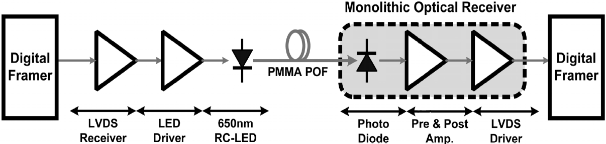
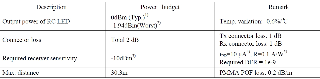
Fig. 1 shows the block diagram of the POF link system. The transmitter consists of digital framer, low-voltage differential signaling (LVDS) receiver, light emitting diode (LED) driver, and resonant-cavity (RC) LED. High-speed POF links above 100 Mb/s require LVDS as an electrical interface. Typical output optical power of the RC LED is 0 dBm at room temperature, and minimum output power is about 0.64 mW(-1.94 dBm) due to temperature effects from -20℃ to 80℃ [1]. PMMA POF at 650-nm wavelength has quite large signal loss about 0.2 dB/m. Therefore, optical sensitivity of the receiver determines the maximum transmission distance. The receiver is composed of PD, pre amplifier, post amplifier, LVDS driver, and digital framer. The optical sensitivity is affected by responsivity of the PD and minimum allowable currents of the pre amplifier for the specific bit error rate(BER). In the POF links, 1e-9 of BER is required. Power budget for maximum transmission distance is summarized in Table 1 [2-4]. In the noise simulation of the pre amplifier,
POF link system
the minimum allowable photo current for 1e-9 BER is 10 μA, and the responsivity of the CMOS PD is measured to 0.1 A/W at 3.3 V reverse bias voltage. The minimum optical power for 1e-9 BER at the input of PD is calculated to be-10dBm with the above parameters. Therefore the maximum transmission distance of PMMA POF link is about 30.3 m.
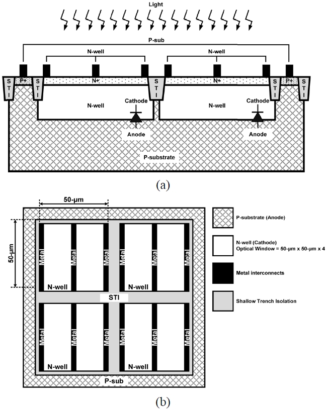
In a standard CMOS technology, there are two possible PN junctions, P+/N-well and N-well/P-substrate. The doping concentration of N-well is larger than P-substrate, that is, the number of minority carriers of N-well/P-substrate junction (holes) is smaller than that of P+/N-well junction (electrons). Therefore an N-well/P-substrate junction can produce much higher photo currents due to its larger drift currents with larger depletion width at nominal reverse bias voltage. However, an N-well/P-substrate photodiode has worse frequency response than a P+/N-well photodiode due to its much longer penetration depth for the diffusion currents [5]. Consequently, an N-well/P-substrate photodiode has better responsivity and worse frequency response than a P+/N-well photodiode. In our application, an N-well/P-substrate is more appropriate due to its high responsivity. Fig. 2 shows cross section and top view of an N-well/P-substrate photodiode. A shallow trench isolation (STI) layer is used for leakage blocking between P+ and N+. To compensate slow diffusion, an N+ electrode is added at the center of each N-well optical window as
well as at the edge. Additionally by separating the photo-diode into four sections each having 50-㎛ by 50-㎛ of optical window, the penetration depth of diffusion currents can be reduced. Many electrodes are of help to improve frequency response, however, the responsivity is decreased because the area of the effective optical window is reduced.
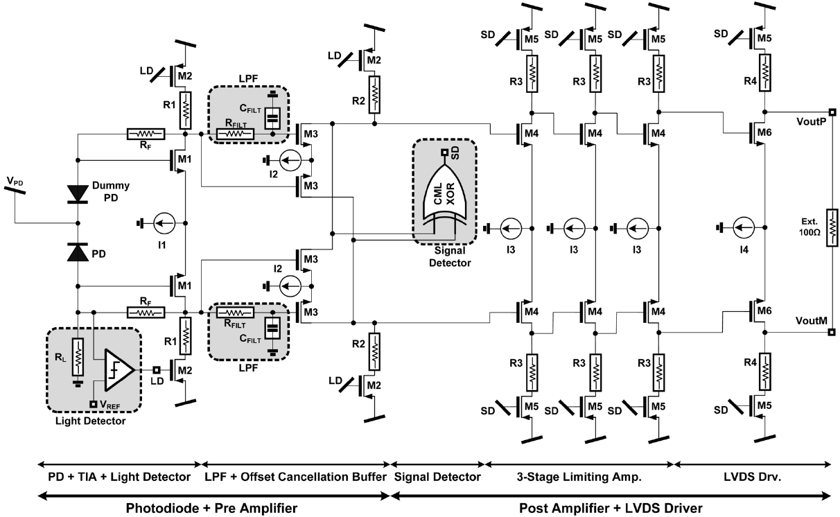
Fig. 3 shows the schematic diagram of the proposed monolithic optic receiver. It consists of PD, dummy PD, trans-impedance amplifier, light detector, low-pass filter, offset cancellation buffer, signal detector, 3-stage limiting amplifier, and LVDS output driver. Dummy PD is added to provide symmetrical input capacitance of the differential architecture as well as to reduce the effect of dark current. The light detector senses whether the light above estimated receiver sensitivity (-10 dBm) comes into the monolithic PD or not. The light detector can be composed of 165 kΩ of resistor(RL), 1.65 V (half of supply voltage) of reference voltage, and comparator. With these parameter settings, input DC voltage becomes greater than the reference voltage when the optical power is more than -10 dBm, and vice versa. In the sleep mode the input resistance saw into gate of M1 is nearly infinite, therefore all of the photocurrent flows through RL. In the other hands, the input resistance of gate of M1 is nearly Rf/(1+gm1R1) in the active mode, so almost all of photocurrent go into the trans-impedance amplifier. All optical receivers cannot have fully differential architecture because the photocurrent comes into only one port. Therefore there are DC offset errors between differential signals due to inherent pseudo-differential architecture. To reduce the bandwidth degradation, an ft doubler with a low-pass filter is used for an offset cancellation buffer [6]. The input capacitance is half compared with a conventional common-source buffer. The pre amplifier has 60-dBΩ trans-impedance gain.
Even if light over the threshold sensitivity is detected, it may have no information, that is to say light may not be modulated. In this case, post amplifier and LVDS output driver don’t need to operate. Therefore the signal detector between pre- and post-amplifiers is added to prohibit unnecessary operation. If the light is not modulated, the differential outputs of the pre-amplifier don’t have a polarity. Thus the signal detector can be easily designed by using an exclusive OR function to detect whether the polarity exists or not. The limiting amplifier consists of three identical common-source voltage amplifiers. For the desired output swing levels(350 mVpp), the limiting amplifier has 32-dB voltage gain and 180-MHz bandwidth. LVDS output buffer drives off-chip 100-Ω termination for LVDS interface.
III. CHIP IMPLEMENTATION AND MEASUREMENT RESULTS
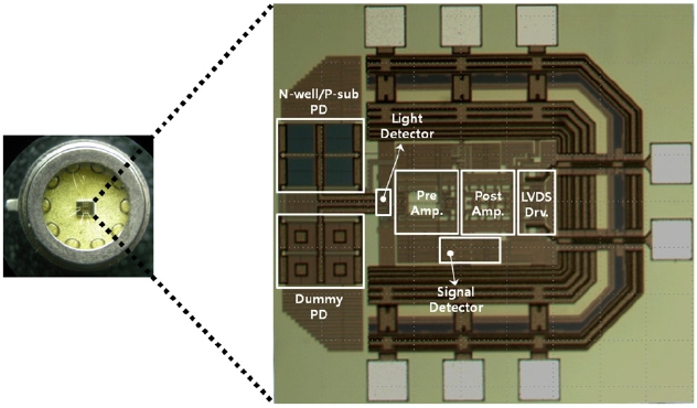
A 150-Mb/s monolithic optical receiver for plastic optical fiber link is realized using a standard CMOS technology. Fig. 4 shows the microphotograph of the prototype TO-can packaged chip. The receiver occupies the area of 765-㎛ by 730-㎛ including electrostatic discharge (ESD) diode
pads. The receiver core dissipates 19.14 mW at a 3.3 V supply.
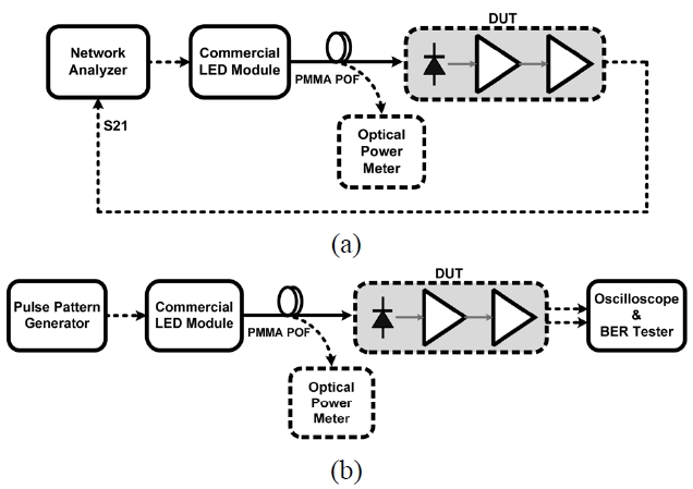
Fig. 5(a) and 5(b) show the measurement setup for frequency and transient responses, respectively. Similar to the practical case, the light from the commercial LED module is connected to the device under test (DUT) through bare step-index (SI) PMMA POF and micro-lens [7]. Alignment between the TO-can package and the POF is manually conducted by an electronic XYZ stage. A well-aligned circumstance is simply judged through spectrum analyzer and radio-frequency signal generators. For a frequency response experiment, a 2-port network analyzer is used, as shown in Fig. 5(a). For measurements of transient response and BER, a pulse pattern generator makes a pseudo-random bit sequence 231-1. Commercial LED driver module converts the NRZ electrical data into optical data with 10-dB extinction ratio, and optical data goes into the DUT. The output waveform can be observed by a sampling oscilloscope and can be com-pared to the input patterns for BER test. Commercial LED module can be used for BER test by controlling the output optical power from -15 dBm to 4 dBm. At the end of PMMA POF, we can observe the incident optical power into DUT by using an optical power meter.
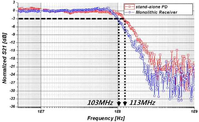
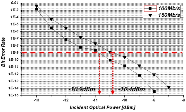
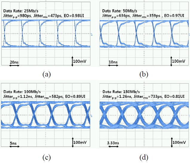
Fig. 6 shows normalized frequency responses of the stand-alone PD and monolithic receiver. For measurement of PD response, stand-alone PD is fabricated with bonding pads. The absolute magnitude value has no meaning in the full optical-link measurement because the measured response contains the response of a commercial LED module. A commercial LED module having 1-GHz bandwidth doesn’t affect the total bandwidth, however, its amplitude response is reflected in the link response. The stand-alone PD and monolithic receiver exhibit 113-MHz and 103-MHz bandwidth, respectively. The stand-alone PD and receiver also have gain flatness under 1 dB. Fig. 7 shows the measurement of BER according to the incident optical power. At 100 Mb/s and 150 Mb/s, -10.9 dBm and -10.4 dBm of optical sensitivities are achieved for 1e-9 BER. The bit rate increases by 50%, however, the difference of BER is only 0.5 dB. The BER limitation is inter-symbol interference due to the lack of bandwidth in 150-Mb/s data rate, while the noise boosting is the BER limit in 100-Mb/s data rate. The eye patterns from 25 Mb/s to 150Mb/s under the condition of -10-dBm optical power are presented in Fig. 8. Above 0.8UI horizontal eye openings are guaranteed for all data rates.
A 150-Mb/s monolithic optical receiver for POF appli-cations is designed, discussed, and implemented. The receiver is fully integrated including CMOS N-well/P-substrate photo-diode. By using light detector and signal detector, power dissipation leakage during no light or no modulation conditions is reduced. The monolithic receiver can successfully detect 150-Mb/s NRZ optical data with -10.4-dBm sensitivity, corresponding to up to 30-m long transmission distance.