Organic solar cells (OSCs) have been intensively investi-gated as one of the promising green energy sources due to the feasibility of producing thin, light-weight, and flexible solar cells [1]. However, the power conversion efficiency should be further improved for practical use of the OSC. Optical interference effects play an important role in the efficiency of multilayer OSCs, where the thickness of each thin-film layer should be carefully designed to maximize the optical absorption in the active region.
The optical interference effect of the multilayer solar cells has been modeled based on the finite element method (FEM) [2, 3], the rigorous coupled-wave analysis (RCWA) [4, 5], and the transfer matrix method (TMM) [6-8]. Among them, the TMM has been widely used for thin-film OSCs due to its relatively ease of simulation code implementation but high accuracy in calculation results. The TMM-based optical model for the OSC provides the spatial distribution of the time-average optical power dissipation
Recently, the angular response of thin-film OSCs with respect to the incidence angle of sunlight has been intensi-vely investigated due to the fact that most OSCs, having the advantage of low-cost production and flexible appli-cation,are expected to be used without a sunlight tracking system. The TMM-based optical model for normal incidence has been adopted for oblique incidence to analyze the angular response of thin-film OSCs [9-11]. However, the previous TMM-based optical models for oblique incidence of sunlight are still insufficient.
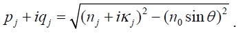
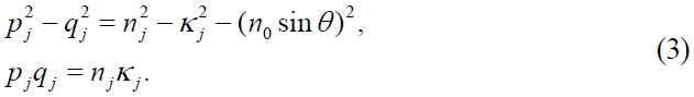
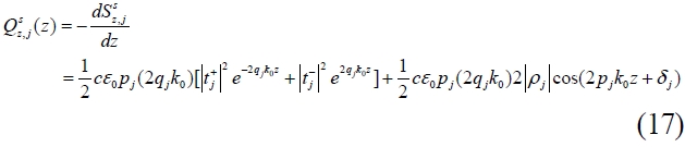
It was mathematically proved that
In this paper, we present comprehensive optical modeling and calculation results of thin-film OSCs at oblique incidence of sunlight. By applying the TMM at oblique incidence, we derive a simple expression for
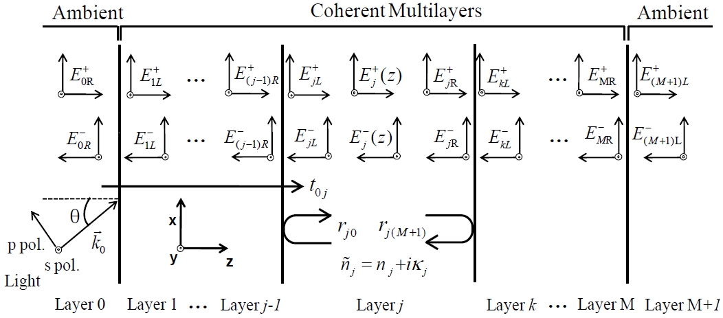
Fig. 1 shows a stack of M layers, where a plane wave with an incident angle
where
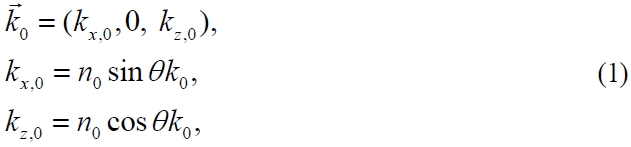
In Fig. 1, the wave vector in the transparent ambient of the 0-th layer is given by
where
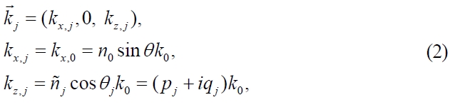
where the relation
and
correspond to the effective refractive index and the extinction coefficient for the z direction. From the dispersion relation
we have
Consequently, we obtain
2.1. Internal Reflection and Transmission Coefficients in Layer j
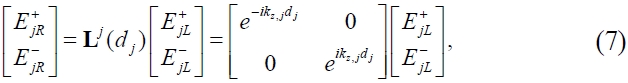
In Fig. 1, we assign a positive (negative) direction to the light propagating from left (right) to right (left), designating the + (-) superscripts. The electric field amplitudes on the interface between the adjacent layer j and k=j+1 are described by an interface matrix Ijk:
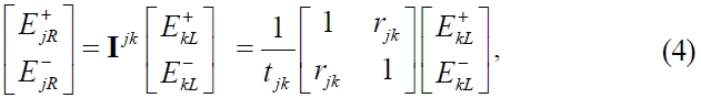
where

and

are the forward-propagating electric field amplitudes at the right boundary of the layer j and the left boundary of the layer k, respectively. The terms
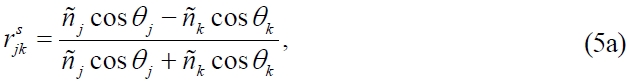
and for p-polarized light as
The propagation of the electric field amplitude between the left and right boundaries of the j-th layer is described by a layer matrix Lj:
where we assume the time dependence of eiwt.
In Fig. 1, the electric field amplitude passing through all the M multilayers from the ambient on the left (layer 0) to the right (layer M+1) can be written as
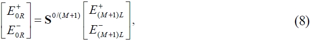
where the amplitude scattering matrix S0/(
If there is no incidence of light from the ambient on the right (layer M+1) to the left (layer 0),
and the front-reflection and front-transmission coefficients from the layer 0 to M+1 can be obtained by
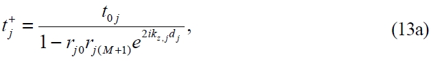
In the same manner, we can define the complex reflection and transmission coefficients for the j-th layer in terms of the matrix elements
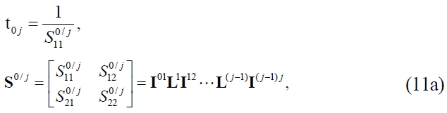
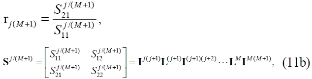
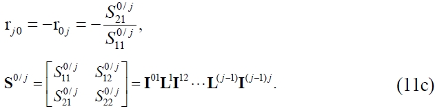
As shown in Fig. 1, t0j is the internal transmission coefficient from the ambient on the left (layer 0) to layer j. The terms rj0 and rj(M+1) are the internal reflection coeffi-cients through the partial front multilayers from layer j to layer 0 and through the partial rear multilayers from layer j to layer M+1, respectively.
2.2. Optical Power Dissipation for S-polarized Light
The y component of the electric field in the j-th layer is expressed as
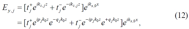
where

is an internal transfer coefficient, relating the incident plane wave to the internal electric field propagating in the positive (negative) z direction at the interface between the layer j-1 and j [13]. The values of

and

are given by

where t0
The time-average Poynting vector in the z direction is expressed as
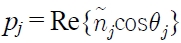
where we can define
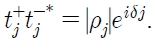
Finally, the optical power dissipation in the z direction is given by


where
and
2.3. Optical Power Dissipation for P-polarized Light
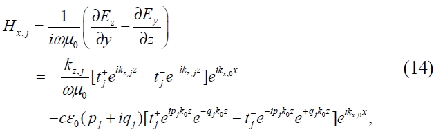
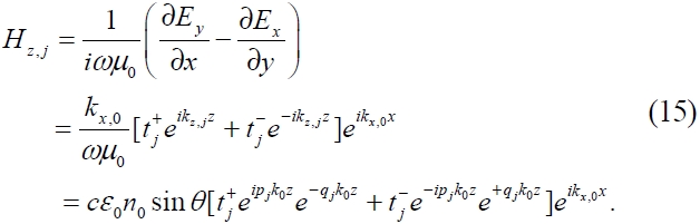
The x and z component of the magnetic field in the j-th layer can be written as
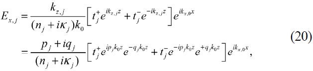
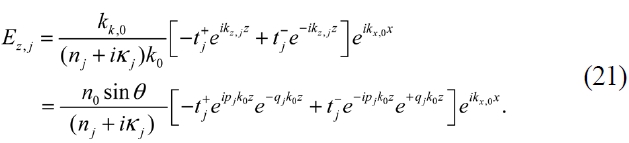
The corresponding magnetic field is given by
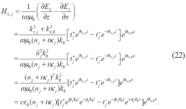
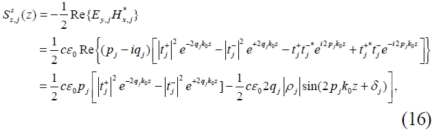
The time-average Poynting vector in the z direction is given by
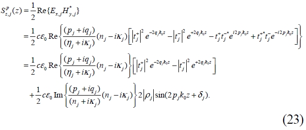
Finally, the optical power dissipation in the z direction is written as
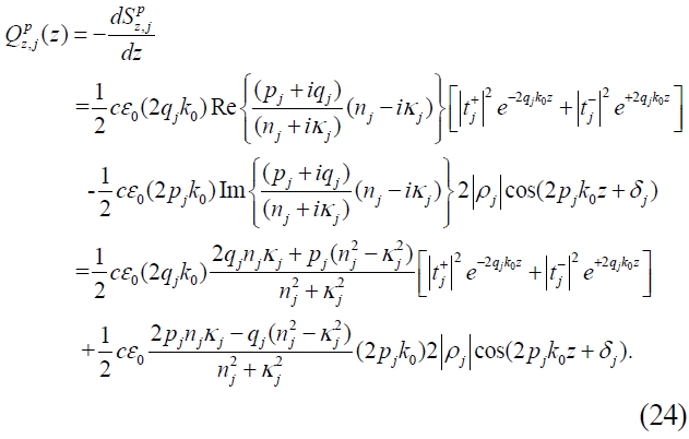
Rearrangement of Eq. (24) together with Eq. (3) leads to
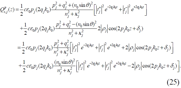
By substituting the expressions for Ex,j and Ez,j in Eqs.(20) and (21) into Eq. (25), we obtain
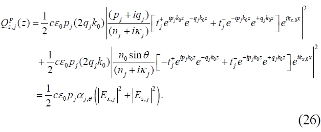
It is remarkable that the optical power dissipation for p-polarized light at oblique incidence is also proportional to the electric field intensity, which is composed of the x and z components of the electric field amplitude for p-polarized light. Thus, information on the electric field intensity with respect to light polarization and incident angle is sufficient to calculate the optical power dissipation in the OSC.
2.4. Total Light Absorptance at the Active Region
Because light absorbed in the active region of the OSC can contribute to the electric power generation, we have to maximize the light absorption efficiency at the active region to enhance power conversion efficiency of the OSC. The light absorptance of the layer j (dj-l≤
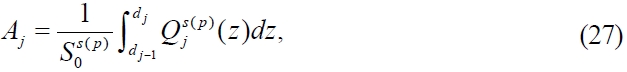
where

is the optical power of sunlight light with s(p) polarization, which is incident from the ambient on the left.
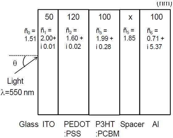
Fig. 2 shows the multilayer structure of the OSC along with its corresponding complex refractive index, which is
taken from Ref. 14. The wavelength of light is assumed to be 550 nm, where the P3HT:PCBM active layer has a peak absorption. We consider the incident angles of 0°, 30°, 45°, and 60° in this calculation. The thickness of the optical spacer layer is varied as x = 50, 100, and 150 nm to adjust the optical interference effect and maximize the electric field intensity distribution within the active region.
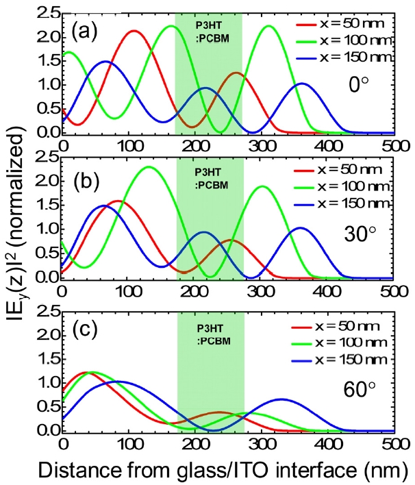
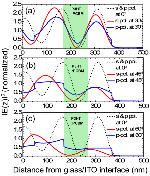
Fig. 3 shows the y component of the normalized electric field intensities at the spacer thickness of 50, 100, and 150 nm. The light green area in the middle of Fig. 3 indicates the P3HT:PCBM active region, where the electric field intensity distribution is important for determining the efficiency of the OSC. The value of the electric field intensity is normalized to s-polarized light incident from the transparent glass on the left ambient when the incident angle is (a) 0°, (b) 30° and (c) 60°. From the ITO toward the Al layers, the oscillating electric field intensities show the general inter-ference pattern [6-8]. For normal incidence (
becomes smaller at the larger incident angle.
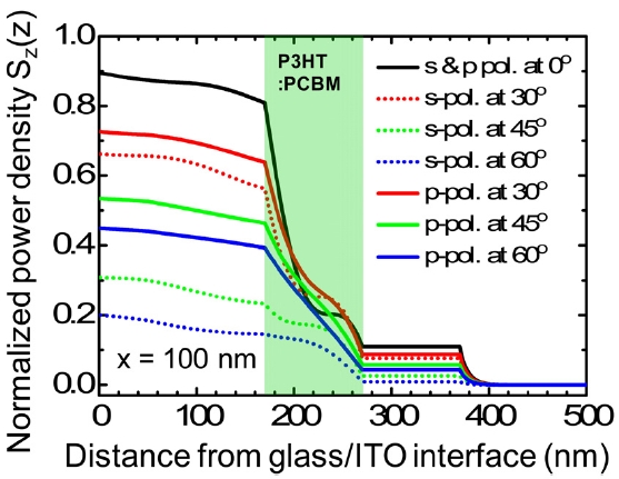
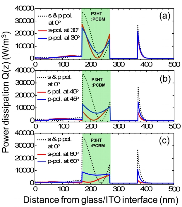
Fig. 4 shows the time-average Poynting vectors
vectors are normalized in reference to the incident optical power from the transparent glass. As the incident angle increases, the value of Sz(z) at the glass-ITO interface (z = 0 nm) decreases because the front-reflection coefficient of the OSC multilayer, r0(
Fig. 5 shows the comparison of the calculated normalized electric field intensities between s- and p-polarized light at the incident angles of (a) 30°, (b) 45°, and (c) 60°. For reference, the normalized electric field intensity distribution at normal incidence is shown in the black dotted line. The optical spacer layer thickness is x = 100 nm. The electric field intensity for p-polarized light |
the incident angle. According to the definition of light absorptance in Eq. (27), p-polarized light shows the relati-vely higher light absorptance in the P3HT/PCBM active region than s-polarized light does This is more pronounced as the incidence angle increases from 30° to 60°.
We presented comprehensive optical modeling and calculation results of thin-film OSC at oblique incidence of light. Based on the TMM, the simple expression for the optical power dissipation was derived at oblique incidence for s- and p-polarized light. Depending on light polarization, we calculated the spatial distribution of the electric field intensity, the timeaverage Poynting vector, and the optical power dissipation at various incidence angles. As the incidence angle increases, the optical power dissipation in the active region becomes smaller for both s- and p-polarized light. In the P3HT/PCBM active region, p-polarized light shows relatively higher light absorptance than s-polarized light does. This is more significant as the incidence angle increases up to 60°. We expect that our optical modeling results help to design more efficient OSC with light absorption efficiency improved,considering the optical interference effect of the OSC at oblique incidence.