An EO/IR optical system that was supposed to be mounted as a payload in an airborne system was designed to satisfy a certain set of requirements. Main requirements were outer dimensions defined to place the system in the allocated volume, resolving power that depended on both optical characteristics and image quality, and functional durability in the extreme environmental conditions. This system was comprised of various components including a yoke, a housing, a gimbal for stabilization, an EO/IR sensor and an optical window for dual band. The EO/IR sensor of the system was designed to provide high-resolution images by thermal IR at night and by visible (EO) in daytime, or by both simultaneously at far-off ranges[1-2]. It was mounted on a two-axis gimbal that provided stabilized imaging and precision pointing in both along the track and cross-track directions.
The optical window was positioned on the outer cover of the payload. The purpose of this optical window was to provide a clear aperture for the desired radiations (Visible and Infrared) while keeping the EO/IR sensor protected from the outer harsh environment. Thus, it was essential that it be able to bear any atmospheric changes such as temperature and pressure because this system was supposed to be operated at high altitude [3].
This paper described the methods for determining the theoretical requirements of the large (413 mm × 313 mm × 15 mm) multispectral window (transmits both visible and infrared) employed for the airborne camera’s primary sensor system. The requirements derived were verified by measuring the image resolutions during the fabrication and evaluation stages. We measured every possible deformation at every step from fabrication to assembly (bonding, bolting) because the optical system was very sensitive to deformation in this system, and those were compared with the calculated data from the simulation performed previously to define the requirements.
II. WINDOW REQUIREMENTS AND SPECIFICATIONS
2.1. Requirement and Specifications
Detailed specifications for the final coated DBW were developed based on the operational requirements of the EO/IR camera system and the optical performances of the EO/IR sensor. To determine the requirements, a great deal of consideration was required because it was the first attempt to use a ZnS (Cleartran) window with diameter 400mm for dual band in Korea. The primary requirements for the design and fabrication of the ZnS (Cleartran) window for dual band can be summarized as follows.
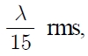
Just like the primary and secondary mirror features, which were optically very critical in the high-resolution reflective optics, the wavefront deformation of the DBW was also a very important parameter for achieving the high-resolution image quality. In this report, the surface figure error of the DBW was defined by transmitted wavefront deformation (TWD) as λ/15 rms at 632.8 nm across 11-inch aperture. This was determined as manufacturing error value and derived through WFE allocation.
The required optical MTF value was provided by the system allocation process. System optical MTFs, including all the degradation factors listed below were 0.3(EO)/0.2(IR).
- Optics Manufacturing Error
- Design + Alignment Error
- Assembly Error
- Environmental Error (Gravity, Temperature etc.)
- Other (Interface, Unknown factors, etc.)
Nevertheless, the MTFs were not convenient parameters for performance analysis. Therefore, these allocated MTF values were translated into WFE degradation parameters. The rms WFE was the most convenient parameter to quantify the optical image quality degradation obtained through several types of analyses (thermal, mechanical and optical). The Shannon formula was used as a tool to obtain rms WFEs from the allocated MTF degradation values [4-5]. The Shannon formula is described in Eq. (1)
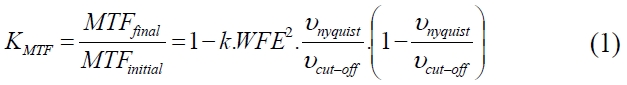
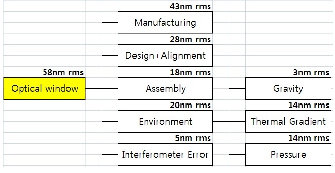
where the k-factor that is dependent on the type of aberration was determined based on previous experience. Fig. 1 shows a list of rms WFE item allocation for the DBW.
The Design + Alignment parameter was residual assembly/alignment error on the window wavefront, mainly due to the assembly of optics with structure, according to the tolerances allocated for each component. The expected performances were derived from initial assembly and manufacturing errors such as follows : Wedge angle (6 arc-sec), Thickness (±0.3 mm), Decenter (±0.5 mm), Tilt(±0.5°), Position(±0.3 mm).
The performance predicting simulation was carried using the Code-V macro. We made a displacement error occurrence macro so that we could input values within the tolerances for the 5 items mentioned above. Within ±2σ(95.4%) ranges, which were derived by performing 1000 times in the macro, we obtained optimum prediction performance results for a given optical product by taking into account the various displacement errors that occur in mass production[6-9]. The Assembly parameter could be induced during assembly of the structure as well as during stress release after mounting. Expected performances for bonding effects were derived by the pilot test between two sheets of BK7 glasses of the same size as the ZnS window and frames. The deformation from bonding effects was 12.7 nm rms at each surface.
The Environment parameter represented the optical com-ponents, the mechanical interfaces and the structures. Analysis was performed for three considerations : Gravitational effect (induced by 1G gravity since the system was assembled and aligned on ground but would be used in the air. It concerned both the structure and the optics), thermal gradient effects (induced by the temperature differences between inner and outer surfaces at the optical window during the operation), and pressure difference effects(to investigate these effects, analysis was performed within the pressure range of 1 Kpa ~10 Kpa). The predicted optical performances in the cases considered above were then analyzed using the Zernike polynomial decomposition method.
Eventually, Manufacturing error (λ/15 rms at 632.8 nm) was determined as differences between total window budgets to satisfy the system MTF and the sum of optical allocation values (Design + Alignment, Assembly, Environment and Interferometer errors).
As shown in Fig. 1, the Manufacturing parameter was the largest among the optical budgets, so we should seriously consider putting more effort into the fabrication of this window.
The window should be large enough so it can secure the F.O.V of the sensor in order to satisfy the required image coverage requirement.
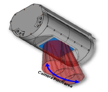
A forward motion compensation scheme was mechanically implemented to eliminate image smear due to the platform’s forward motion [10]. The gimbal inside the payload was designed to rotate the F.O.V in pitch direction up to ±15° as shown in Fig. 2.
Since the outer gimbal that the window was mounted to did not include the driving mechanism, the window should be expanded further in pitch direction in order to secure the camera’s field of view.
The design of the DBW was iterated 3 times, reflecting consider-ations of the operation concepts of the gimbal. Optimized window configuration and analysis results are shown in Table 1 below. The window thickness was selected based on a structural analysis using a simple edge-supported model of the window installation, and 15 mm thickness was selected for the DBW.
Initially, a window that has octagon shapes with 600 mm × 400 mm dimension was designed, but the concentrated stress that occurred at the edge area was shown in the 1st
[TABLE 1.] Optimization of the DBW
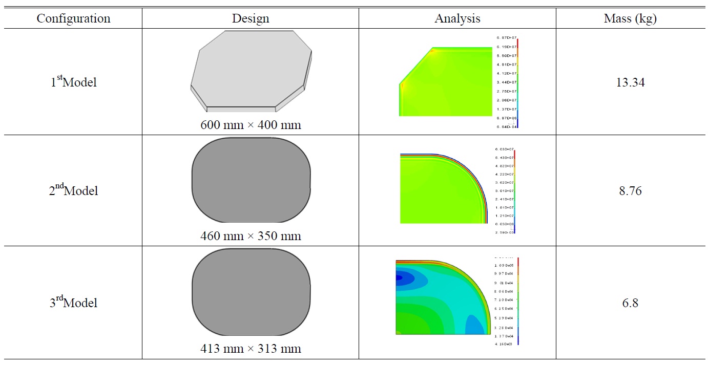
Optimization of the DBW
Model of TABLE 1 above. In order to reduce the stress concentration at the edge of the window, it has been modified from an octagonal shape to a rounded one. The revised window of 460 mm×350 mm shown in the 2nd Model of TABLE 1 above had uniformly distributed stress and reduced volume and weight. The reduction rates of the volume and weight were 30% and 50%, respectively.
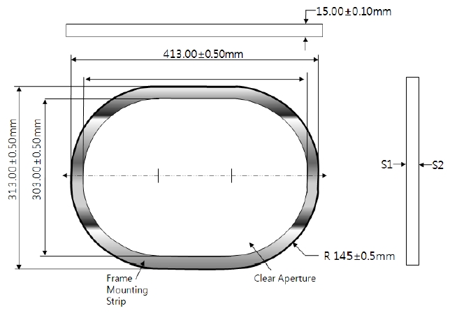
Although both inner and outer gimbals could be driven in the roll direction during scanning, there was a possibility that their rotation angles did not match exactly. The roll angle errors for the inner and outer gimbals were estimated as from ±2° to ±1° by considering the system’s dynamic characteristics. Therefore, another ±1° should be added to the maximum roll angle range. An optimized optical window that secures the camera’s field of view was finally designed after considering this limitation in addition (3rd Model in TABLE 1). Size 413 mm×313 mm and edge radius of 150 mm were selected as the finally designed DBW configuration, which can be seen in Fig. 3. The 3rd Model is about 50% the weight of the 1st Model. The 3rd Model shows light weight effects of about 50% compare to the 1st Model.
3.1. Measurements of the Optical Quality of CVD ZnS
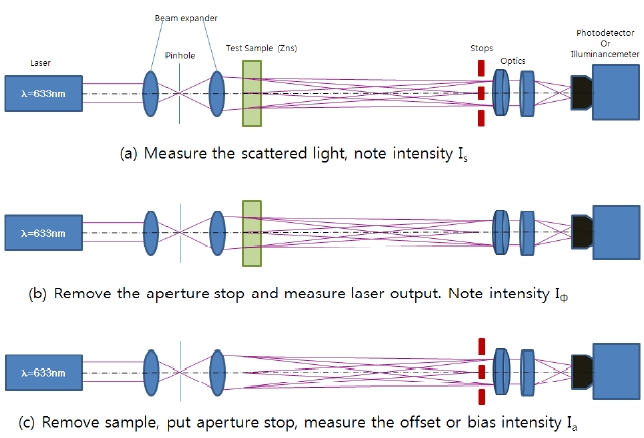
ZnS (Cleartran) is a wide-band optical material and is one of the most widely used IR optical materials due to its good mechanical and thermal properties and theoretically excellent optical performances. It is known that bulk ZnS produced by CVD growth is very sensitive to the machining process[11-13]. Forward Scatter was selected as the inspection
method to control the degree of clarity of ZnS raw material.The procedure of the Forward Scatter method is as follows;
1. Put the ZnS sample just after the beam expander.
2. Measure the scattered light intensity IS. (Fig. 4(a))
3. Remove the stop and measure the laser output. Note the intensity signal IΦ. (Fig. 4(b))
4. Remove the sample and put the stop in the detector unit. Repeat again step 2 and measure the offset or bias intensity Ia (Fig. 4(c))
5. Calculate the scattered light ratio as follows:CS = {(IS ? Ia)/( IΦ)}x(1/d) (Normalized on the sample thickness d(cm))
Forward scatter measurement results were below 5%/cm.
3.2. Fabrication of the Optical Window
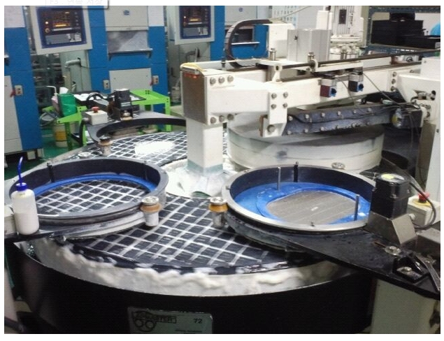
We fabricated the DBW using the selected ZnS material. The critical requirements of the window were that TWD error should be less than λ/15 rms, and the wedge also should be less than 6 arc/sec with surface quality (scratchscatter/dig) better than 60/40. We first attempted a conventional polishing method with pitch tools and diamond slurry for final polishing.
Even though we obtained P-V value less than one lambda for every 11.8” diameter clear aperture for each side of the window, the asymmetrical shape of the window made the TWD error worse than λ/3 rms. The fringe analysis result showed us that the TWD error is 1.65 λ RMS for the worst case for the conventionally polished window. In order to measure the quality exactly and to obtain feedback for the polishing process, we installed a new 12” interferometer.
As the window was quite thin (thickness was 15 mm) relative to the size of the window (length was 413 mm on one side), normal jigging of the window might cause stress on the window. So, we used stress free polishing with 72” Lapmaster equipment shown in Fig. 5. The result showed us better value λ /3 rms, but still didn’t meet the requirement.
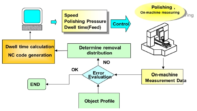
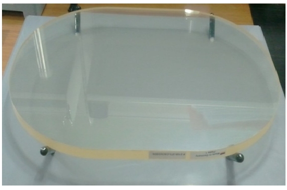
To secure TWD quality less than λ/15 rms, we performed conventional polishing followed by Lapmaster polishing. After those processes, we carried out correction polishing as described in the diagram below (Fig. 6). An in-situ 300 mm diameter Fizeau interferometer was developed additionally and used to monitor TWD error of the window in real time. Finally, the polished window showed us TWD less than λ/15 all over the whole clear aperture. Fig. 7 shows the configuration of the finally fabricated window.
3.3. Evaluation of the EO Camera Resolution by the Transmitted Wavefront Deformation (TWD)
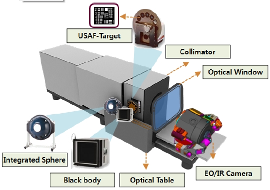
In this section, we explain the evaluation process of the EO camera resolution performance according to the transmitted WFE levels. Fig. 8 shows the equipment set up for image acquisition to measure the transmitted WFE levels
The optical window was installed between the EO/IR camera and the collimator (4 m). The effect of imaging resolution according to the transmitted wavefront deformation (TWD) levels was confirmed by comparing the image before and after this window installation.
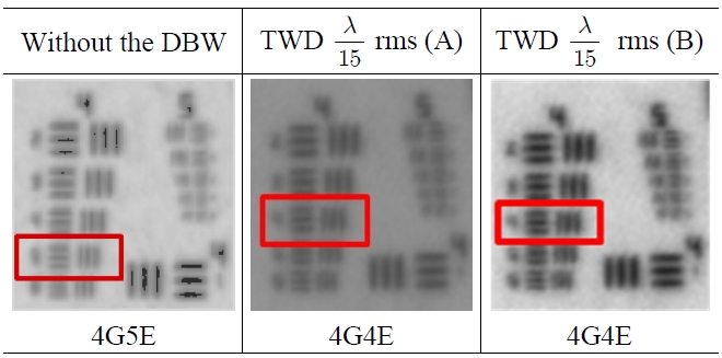
Table 2 shows the image performance for the DBW’s TWD levels from λ/3 rms to λ/8 rms. The required resolving power of the EO camera with the optical window was 4G3E~4E in the USAF 1951 chart. The measured resolution of the EO camera with window that was fabricated with TWD λ/8rms was 4G1E(4Group 1Element). These results showed about a 2~3E(Element) drop compared with the required resolution.
Table 3 shows the resolving power, which is 4G4E in the USAF-1951 chart over any aperture at transmitted WFE

(A) and (B) are window dimensions shown by rotating pitch direction(±15°). These results were sufficient to satisfy the requirements of this system, and indicated that the initial conditions for transmitted WFE were set up correctly. This method can be used efficiently to define
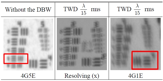
EO camera resolution according to the DBW’s TWD levels (the fabricated DBW did not include a coating)

Image resolution test results of the EO camera (@TWD rms) (the fabricated DBW did not include a coating)
the surface form error levels for the development of large aperture optical windows.
We measured all possible deformations at every step from fabrication to assembly (bonding, bolting), and the results were compared with simulation data which were previously performed to define the requirements.
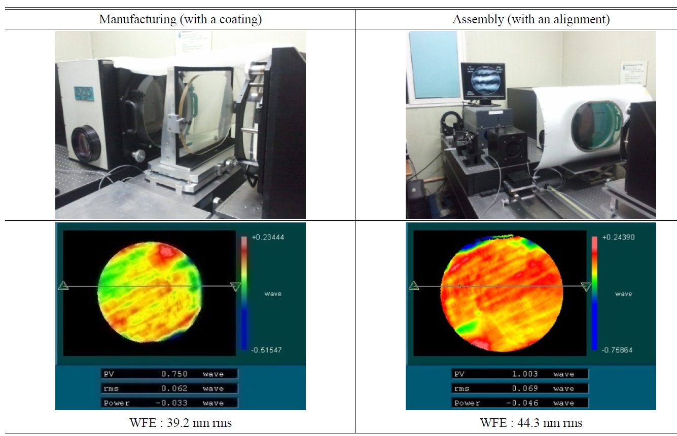
Table 4 summarizes the equipment configuration for testing of the TWD, and shows fringe data at every step. The TWD for the manufacturing (including a coating) and assembly (including an alignment) were 39.2 nm rms and 44.3 nm rms, respectively. These results showed that the series of procedures from fabrication to assembly could be performed well compared with the expected data. The predicted simulation performance results for the fabrication (including a coating) and assembly (including an alignment and an interferometer error) were 43 nm rms and 54.6 nm rms (refer to Fig. 1).
The gasket was bolted at the edge of the DBW, which bonded with the outer cover. 3 step measurements were used to obtain the image resolution influence due to the window with bolted gasket. The first step was to measure the assembled EO/IR camera with only the gimbal (without the DBW). In the second step, the outer cover with the bonded window was added to this camera. The final step was to include the bolted gasket additionally. Table 5 shows this step and those image resolutions from the USAF-1951
[TABLE 4.] WFE measurement result at each step of the process

WFE measurement result at each step of the process
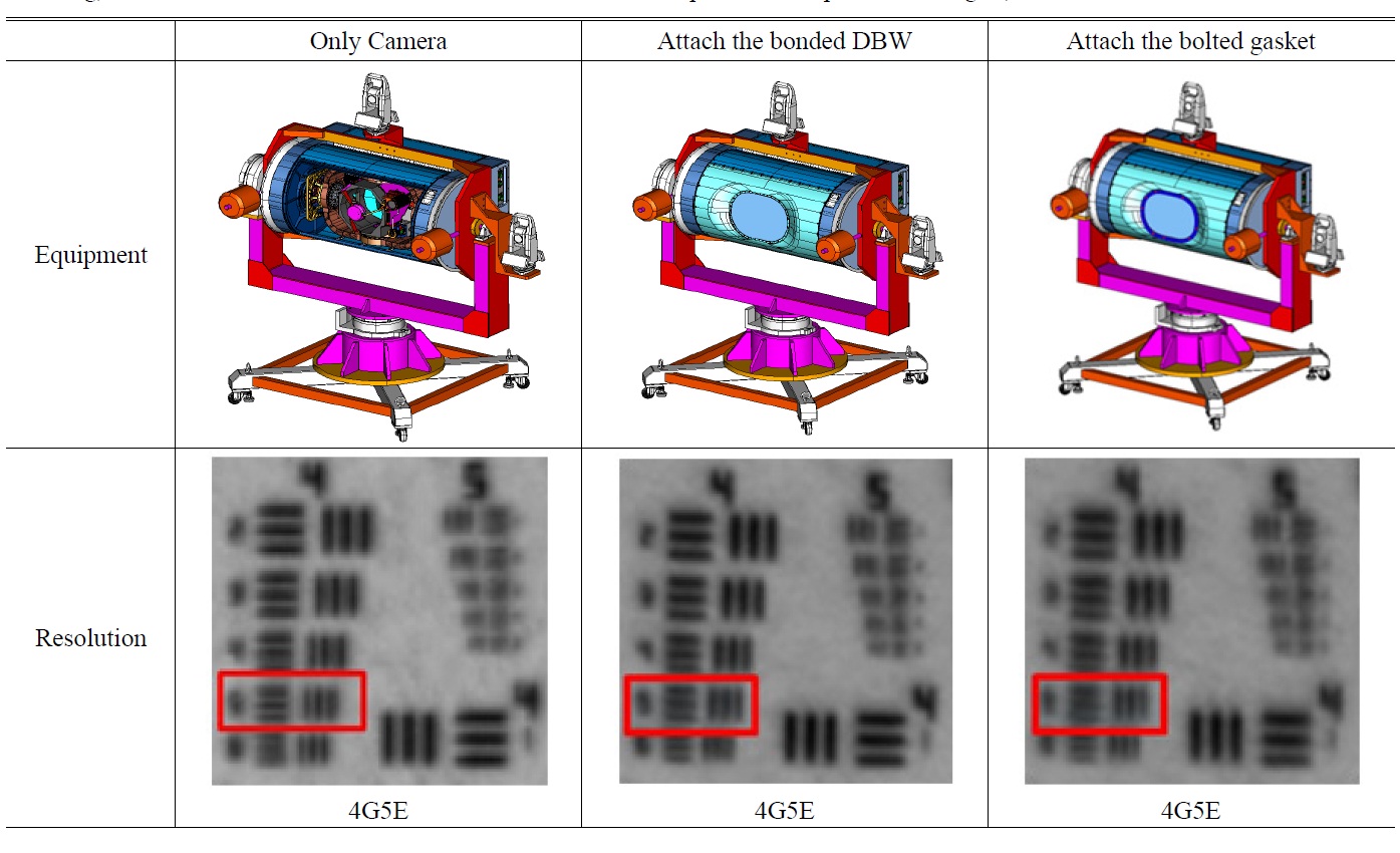
Resolving power at every step from bonding to bolting. (in this experimens we considered only the assembly(bondingbolting) work influence without environment effects such as temperature and pressure changes.)
chart. Image resolutions before and after installation of the optical window were 4G5E in USAF-target, which means that there was no image degradation caused by the DBW.
This article presents a method that could be used to derive the theoretical requirements for the development of a 400 mm optical window with a stable structure. This article also shows the design and fabrication result. A light optical window was designed to secure the image for the camera and to ensure mechanical stability. The optical window was fabricated with the precision derived from the requirements (Transmitted Deformation Wavefront,
The image resolution was verified in each step of the processing
The image quality was not reduced if the precision reached


showing that the detailed requirements were properly satisfied.
Deformation that occurred in the series of fabrication steps, including processing, coating, assembly and bonding, was accurately measured and compared with the result of the simulation that had been performed to derive the predicted performance. The measured results were 39.2 nm
44.3 nm rms for manufacturing and assembly, which was much better than the predicted simulation performance result for assembly, 54.6 nm rms. Finally, we examined the effect on image resolution of bolting when the optical window was attatched to the outside of the payload. The results were 4G5E before the optical window attachment, 4G5E after the optical window attachment and 4G5E after the gasket bolting to the optical window rim.
These results showed that the series of steps from the derivation of the perfomance requirements of the optical window to the fabrication and assembly could be performed well without reducing the target resolution of the system (4G5E). This method is expected to be used efficiently for the further development of large-aperture optical windows