The ring laser gyroscope(RLG) is an important sensor for the Inertia Navigation System. RLG is a type of Sagnac interferometer which measures the rotation angle of the system. Most of the RLG has triangular or rectangular shape and each of the corners of RLG has high reflectance mirrors. According to the theory of oscillators, coupling between the two counter propagation waves can lead fre-quency synchronization, which is called lock-in, and the mirror scattering is closely related to it. The high reflectance mirrors must have very low scattering loss, because of lock-in phenomena in the RLG. And the RLG also needs very low absorption loss to maintain low operating currents, which is a key parameter of RLG lifetime.
Following the Sagnac interferometer theory, the rotation angle of the RLG is measured by taking the frequency difference between the two counter-propagation waves. When the sensor rotates Ω, the frequency difference Δν is given by
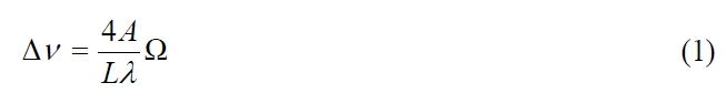
where A is area of the sensor, L is the perimeter length of the RLG and λ is the wavelength of the laser as shown in [1]. The term (4A/Lλ) is called the scale factor of the RLG, and usually it is constant while calculating the angular rotation. To keep the scale factor as a constant, the perimeter of the RLG should be maintained constant while the sensor operates over a wide temperature range. Therefore there are actuators which compensate the perimeter change as the temperature varies. Also, to minimize the perimeter length change while the temperature changes, the RLG body is made of glass ceramic, which has a very low thermal expansion coefficient. Zerodur is one of the glass ceramics which is manu-factured by Schott Corporation. Usually, the mirrors are attached to the body of the RLG by an optical contact method as described in [2], which is a kind of bonding method without bonding material. To maintain the optical contact without contact stress while the temperature changes, not only the RLG body but also the mirror substrate should be of the same material. Therefore the mirror should be fabricated on the Zerodur substrate. But it is very difficult to make the Zerodur extremely flat because of its crystalline structure. Most of the RLG is manufactured based on a He-Ne laser. In the case of the He-Ne laser, the He and Ne plasma is used for the pumping mechanism. He-Ne plasma radiates UV light and it could break the chemical bond of the mirror fabrication material. This mechanism is called UV degradation. If UV degradation occurs in the RLG, the laser cavity loss increases, and the operating current should also be increased.
A few studies report about the low loss high reflectance mirror development in references [3-5], but there is no report about the low loss high reflectance mirror on low thermal expansion material. Zerodur is a composite of ceramic material, which mainly consists of silica and alumina, and it has crystalline structure. In this paper, we develop a high reflectance mirror, which has more than 99.995% reflectance, on the Zerodur substrate, and we study its optical properties.
II. MIRROR DESIGN AND FABRICATION
RLG operates at the red He-Ne laser wavelength with s-polarized light. Therefore the mirror should be designed at the 633 nm wavelength and the angle of incident at 30 degrees for triangular type RLG or 45 degrees for rectangular type RLG. He-Ne plasma emits UV radiation between 300~400 nm range as described in reference [6] and the photon energy in these UV region is 3.1~4.1eV. In this paper we design a mirror for rectangular shape RLG. In this wavelength region, silica(SiO2) is used as a low index material and it has relatively high chemical binding energy(~7eV). TiO2, HfO2, Ta2O5, and ZrO2 are the candidates of high index material. Among the high index material candidates, TiO2 is the highest index material and can be easily made high reflectance. But the TiO2 is relatively high absorption material and it has ~3.5 eV binding energy, therefore if we make the high reflectance mirror using TiO2 as a high index material then the mirror has relatively high absorption and the chemical bond could be broken by the UV plasma of He-Ne. HfO2 and ZrO2 show relatively low absorption, but these are commonly crystalline structure. This means that if we deposit the mirror using these materials, the mirror has large volumetric scattering. On the other hand, Ta2O5 has low absorption, amorphous structure and its chemical binding energy is 4.2 eV as shown in reference [7]. Therefore if we use Ta2O5 as a high index material, the mirror will have low absorption and low scattering. Therefore we choose SiO2 and Ta2O5 as low and high index materials, respectively.
The high reflectance mirror can easily be obtained from a stack of quarter wave layers of alternate high and low index material as shown in [8]. The choice is which material is firstly deposited on the substrate. C.K. Hwangbo solved this problem in [9], which says that when the high index material is deposited as the first layer, the mirror absorption is quite low as compared to the case of the first layer of low index material. The mirror structure that we finally adopted is,
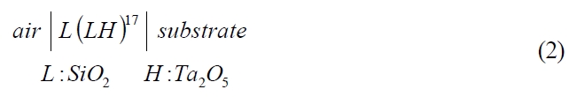
where, L denotes the quarter wave optical thickness layer of low index material and H denotes the quarter wave layer of high index material. In optical thin film design, the half wave layer is used as an absentee layer, where it does not affect the reflectance property at the center wave-length. Since the silica has high chemical binding energy, we insert additional quarter wave low index material in the air interface for UV protection. We also checked the stability of the mirror design, and the reflectivity was stable while the thickness of each layer varies within 5%.
Mirror scattering has two parts, one is the surface scattering which comes from the irregularity of each material interface and another is the volume scattering which comes from the thin film microstructure as described in reference [10-11]. Therefore the surface quality of the substrate is an important factor to reduce the surface scattering. The super polished substrate, which has the surface roughness of less than 0.4 A in rms, was purchased from General Optics Inc.. The surface quality is measured by a phase shift inter-ferometer(PSI)[12], and by an atomic force microscope (AFM) for comparison.
High reflectivity dielectric mirrors were coated by ion beam sputtering(IBS). A Ta target was used as a sputter material to fabricate Ta2O5 films, and 800 eV Ar ions were used as a sputter source with enough backfilled oxygen gas. We used 900 eV Ar ions to directly sputter SiO2 films from the SiO2 target, and introduced small portion of oxygen backfilled gas to supplement the pump-out of oxide from sputtered SiO2. The film thickness and deposition rate were measured by using a quartz crystal thickness monitor. The deposition rate of Ta2O5 film was 1.2 nm/min, and the rate of SiO2 film was 3.6nm/min. The substrate was not heated during the mirror fabrication. To make sufficient oxidation of sputtered dielectric films, the mirror was annealed 7 hours at 450℃ with oxygen ambience.
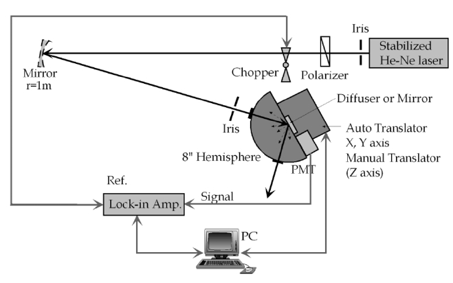
Scattering and transmittance of the mirror was measured by a total integrated scattering measurement (TIS) system, and the mirror loss (= absorption + scattering + transmittance) was measured by a cavity ring-down reflectivity measurement system as shown in [13]. TIS was measured by an internally built TIS measuring system as shown in Fig. 1. A stabilized He-Ne laser was used as a light source, a Glan-Thompson polarizer to make s-polarized light, and the light source was modulated at about 1000 Hz for noise reduction. An 8-inch integrating hemisphere was used for 45º angle of incidence measurements and a PMT as a photo detector. Irises were used to block stray light, which came from chopper and polarizer. For TIS mapping, a mirror was attached to the two axis’ computer controlled auto translator at the right behind the integrating hemisphere.
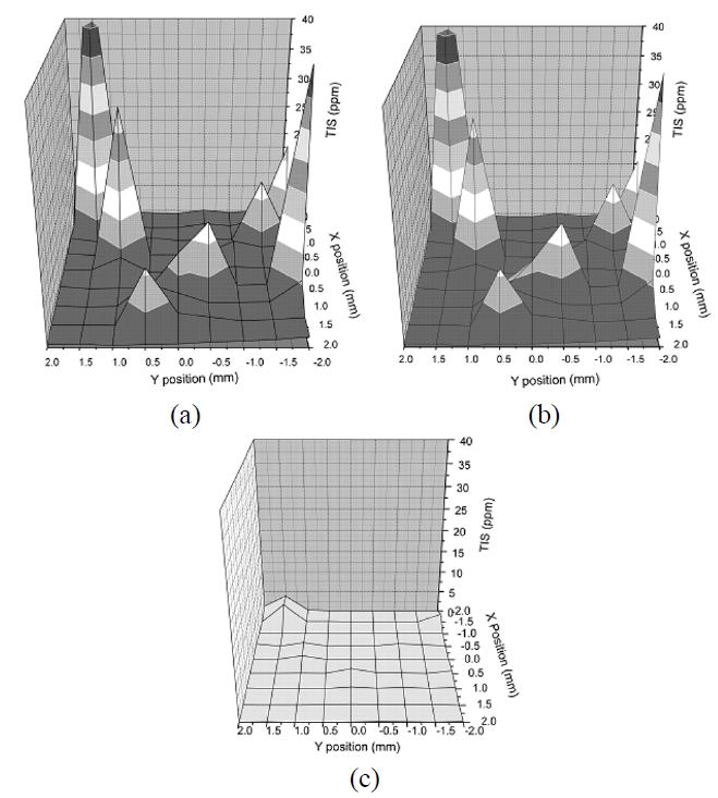
To verify the internally built TIS setup, the repeatability of mirror TIS was measured. TIS mapping had been measured
several times using same mirror and the difference was checked on each mapping point as shown Fig. 2. Fig. 2(a) and Fig. 2(b) show TIS mapping results for the same mirror with two hours time interval, and Fig. 2(c) shows their difference. The maximum difference was 4.5 ppm at the upper left corner of the map. The minimum difference is 0. The mean difference was 0.3 ppm for the whole 81 measured points. We also checked the noise of the TIS setup. The background optical noise was 0.5 ppm and its electric noise was 0.2 ppm.
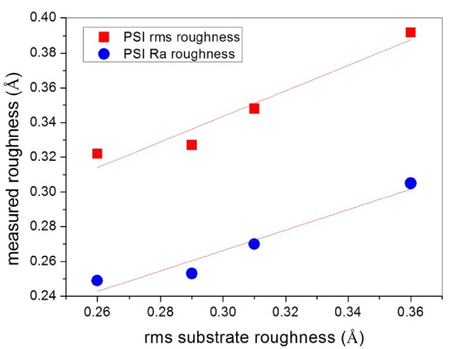
Super-polished substrates were prepared by chemical cleaning and spin cleaning processes, and then the surface quality was measured by PSI using Maxim GP, Zygo. Fig. 3 shows the result of the surface roughness measurement. The measured roughness was a little larger than the manufacturer’s data, and the average surface roughness was a little smaller than as that of rms value. J.M. Bennett and L. Mattsson pointed out in reference [14], if a surface has a profile that contains no large difference from the mean surface level, the rms and average value will be similar. However, if there are appreciable numbers of large bumps or hills, the rms value will be larger than average value.
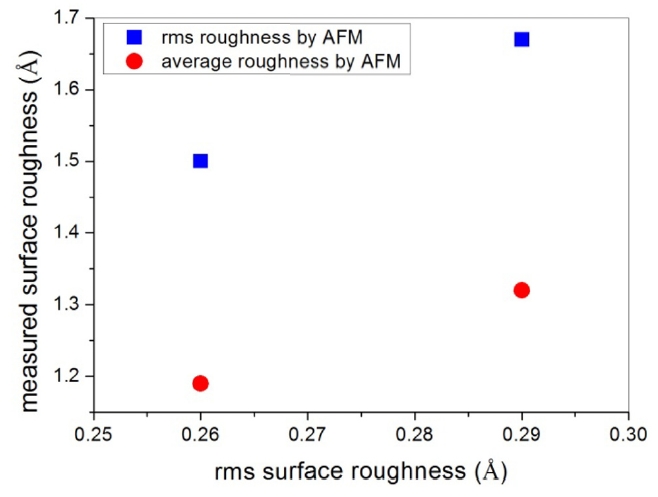
We also used AFM for surface quality measurement and Fig. 4 shows the results of the AFM measurement. The rms and average surface roughness by AFM was about five times larger than the PSI measurement, but it also shows that the rms roughness was higher than the average roughness. This is similar to the result of the PSI measurement shown in Fig. 3. Even though the substrate has a nearly
smooth surface in atomic size, the surface seems to contain relatively large bumps or hills in such a small scale level. And it may be due to the crystalline structure of Zerodur.
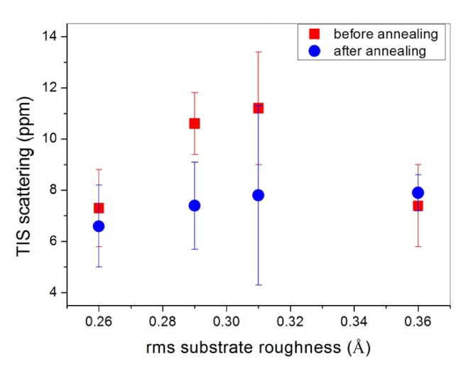
The mirror scattering was measured by the TIS measure-ment system at 45 incidence angle with stabilized He-Ne laser. TIS scattering varies with the mirror position, therefore we measured 81 points within 16 mm2 area and their difference is indicated as an error bar in Fig. 5. The TIS scattering increases as the substrate roughness in rms increases. And TIS scattering before the annealing process was higher than after annealing process, except for the substrate rms roughness of 0.36 A. It could be explain that the mirror has a slightly porous structure or it may have a partly incomplete chemical bond. Though the annealing process, film material may become denser or stably bonded. J.C. Stover mentioned in [15] the relation between the surface roughness in rms and TIS scattering.
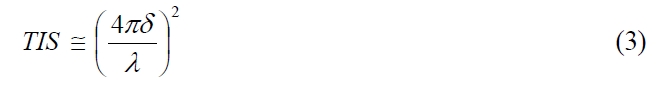
Where, δ is rms surface roughness of the measured surface, and λ is the wavelength of the incoming light. If we calculate the TIS value using PSI measurement results of the substrate, TIS will be around 0.4 ppm. The measured TIS is between 6 to 8 ppm and these are nearly 20 times larger than the calculated TIS. This means that the surface roughness becomes larger while the mirror is being coated. J.D. Rancourt mentioned this phenomenon in reference [16], he said that if there is imperfection in the substrate or bottom side of the multilayer films, the defect grows. As more layers are added to the multilayer stack, the
disturbance caused by the defect increases in lateral extent. We thought that the TIS difference between the calculated substrate and the measured mirror comes from the growing effect.
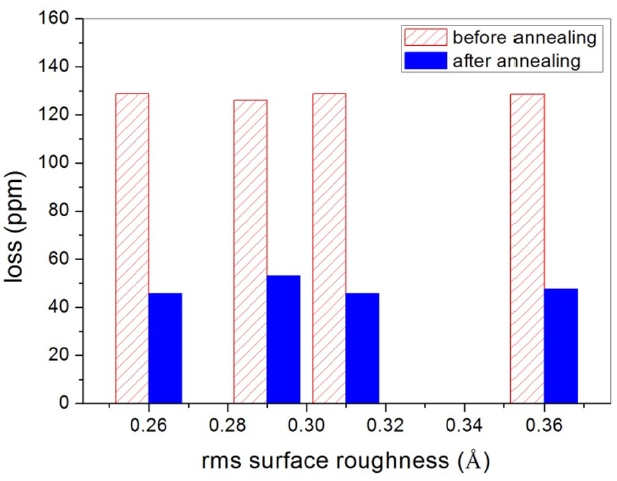
The optical loss was measured by cavity ring-down method before and after annealing as shown in Fig. 6. The measured loss includes scatter, absorption, and the transmittance. Since the transmittance is not an optical loss, we measure the transmittance and then subtract from the measured loss. Therefore the loss is just the sum of optical scattering and absorption. The annealing process decreased the optical losses by two thirds. This means that the scattering and absorption decreased, and as shown in Fig. 5 the scattering decreased up to 4 ppm by the annealing
process. Therefore most of the reduced loss is absorption and it means that there will be chemically imperfect bonds after the mirror coating and these will be changed into perfect chemical bonds while annealing the mirrors. The quantity of the reduced absorption is about 80 ppm. Most of the mirrors have less than 50 ppm loss and such a low absorption means that most of the chemical bond in the mirror will be perfect bonding. As we mentioned in Section 2, the selected material has larger chemical bonding energy as compared to the UV radiation generated from He-Ne plasma.
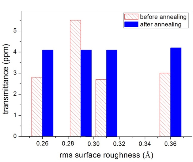
We also measured the transmittance variation due to annealing as shown in Fig. 7. The transmittance was increased by the annealing process except for the case of the mirror with its substrate roughness 0.29A in rms. In metal oxide films, oxidization increases the refractive index and the extinction coefficient decreases. In mirror design, as the refractive index decreases, the mirror transmittance of the reflection region increases. Even though the increased transmittance is very small, this increment during the annealing process means that the mirror-coated material became a stable metal oxide film and the refractive index of the film increased. The optical absorption also decreases during annealing as shown in Fig. 6.
A high reflectance mirror was designed and coated on a Zerodur substrate by ion beam sputtering. Firstly the mirror structure and mirror coating material were carefully selected and devised. The super polished Zerodur substrates were measured by PSI and AFM. The result shows that even though the substrate has very low surface roughness, there might be little bumps or hills, and we believe that these may come from the crystalline structure of the Zerodur composition. TIS scattering of the mirrors was 6-8 ppm after the annealing process. The absorption was about 120 ppm and it was reduced to 40 ppm. Through the annealing process of the mirror, the refractive index and extinction coefficient of the mirror material decreased, and the transmittance increased even though the changed quantity was quite small.