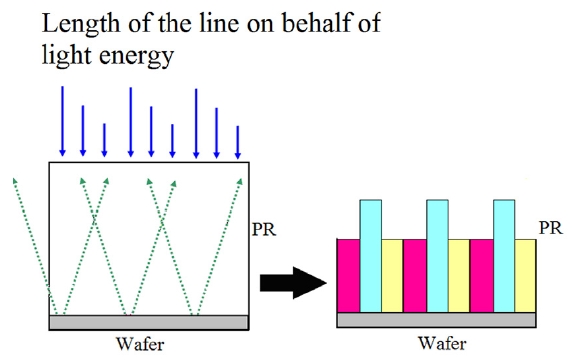
Fresnel zone lenses are fundamental optical components in photonics, optical communication, solar cells, and imaging [1-5]. The final focal length of a Fresnel lens is determined according to the depths and widths of each zone [6-7]. Thus, the manufacturing method must be considered during the design stage. Conventional Fresnel zone lenses are manufactured using laser writing, liquid crystal films, molding, injection, and grayscale lithography [8-12]. Grayscale lithography is an easy way to control the slope of each zone. This approach uses a grayscale mask to expose different areas of the photoresist (PR) to the light of various energies. This method creates a depth pattern that can be used to produce a three-dimensional microstructure quickly [13-14]. Using a physical grayscale mask to fabricate a Fresnel lens requires that all curved surface grayscale values be calculated. This ensures that after development, the exposed surface of the PR has the correct depth and width characteristics [15-16]. This study used three grayscale levels to approximate a curved surface (because additional grayscale levels are necessary to provide surfaces with greater curvatures), and each grayscale level definitively affects the optical quality of the final curvature.
Physical grayscale masks fabricated using conventional methods are expensive, and grayscale lithography is a timeconsuming process. Because grayscale values determine the final depth after development, any errors in the parameters cause considerable losses and negatively affect three-dimensional formability analysis. Thus, many optical lenses require a sample to test the optical quality after design and simulation [17-20]. A maskless lithography system can substantially reduce the cost and time required for grayscale lithography. The grayscale design is easy, accurate, and allows real-time modification of grayscale values [21].
The formability of Fresnel lenses produced using grayscale lithography has thus far attracted little attention. This is primarily because of the laborious preparation required in conventional grayscale mask-employing methods. The grayscale value plays a vital role in the fabrication of Fresnel zone
lenses using maskless lithography, because it has a direct effect on the depth and slope of the Fresnel zone lens. Therefore, with the objective of supplanting physical grayscale lithography with maskless lithography, we investigated the effects of the grayscale value on PR formability. Fig. 1 shows a schematic PR profile obtained using the grayscale lithography technique. Factors determining the final shape of the lens include depth, width, and slope. This paper outlines the maskless lithography system and the production of diverse grayscale masks to obtain various Fresnel zone lenses. This study also provides a discussion of the performance of this method regarding lens parameters.
II. EXPERIMENTAL SETUP AND DESIGN
The amount of light energy absorbed by the PR normally depends on exposure conditions such as the optical properties and photochemical behavior of the photoresist, the resist film thickness, and the reflectivity of the underlying surface. However, considering all exposure conditions is difficult. Therefore, the energy absorbed by the PR can be approximated as J = W × S, where J is the energy absorbed by the PR, W is the energy penetrating the mask, and S is the exposure time.
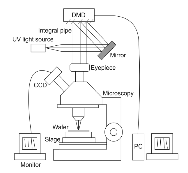
The grayscale mask image is produced by employing a digital micromirror device (DMD) (Texas Instruments). The DMD used in this study is 0.55 in2 and includes 1024 × 768 micromirrors. The size and tilt angle of each micromirror are 10.8 μm2 and ±12°, respectively. The model number is DLP 5500. The horizontal and vertical frequencies of the scanning duty cycle of the micromirror range from15-91.4 kHz and 43-87 Hz, respectively. The switching time of the micromirror is 0.2 ms. The binary pulse width modulation technique (PWM) switches the micromirror and controls the switchtime. Switching the micromirror on and off controls the tilt angle of the micromirror at +12° and -12°, respectively [22]. The switchtime is modulated by the pulse width. A long switchtime produces higher light intensity than a short switchtime does [23]. The viewer’s eye combines the energy and translates the pulses into perceived grayscale intensities [24]. The grayscale level indicates a specific chromatic grayscale level ranging from 0 to 255. The grayscale level was controlled using Microsoft PowerPoint software. The grayscale level 0 indicates the weakest energy, whereas the grayscale level 255 indicates the strongest energy. Different amounts of exposure to UV light lead to different thicknesses of photoresist remaining after development. The thickness is inversely proportional to the light energy. This study provides a discussion on the effects of photoresist formation using different grayscale levels to fabricate a microlevel Fresnel lens.
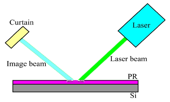
Exposure parameters, such as the soft-baking temperature, time, and sensitivity of the PR to the exposure wavelength, must be considered to determine the final depth of the lithography technique. The substrate is a wafer (Si), and the photoresist (AZ-4210) used in this study was soft-baked at 100℃, with spin speeds of 1500 rpm for 15 s and 3000 rpm for 30 s. The PR was exposed to ultraviolet light, at an intensity of 33 J/cm2 for 60 s. Fig. 2 shows the maskless lithography system, consisting of a DMD-integrated microscope and an ultraviolet light source at a wavelength of 365 nm. The advantage of using microscopy as the optical system is that it can replace the objective lens and eyepiece. In a full-screen (1024 × 768pixel) exposure test, the objective lens is 5x the percentage and the numerical aperture of 0.12 where with a 4x percentage eyepiece to the arrival exposure area of 1 mm2. The eyepiece, with a percentage that is 4x that observed using the microscope, is connected by a charge-coupled device (CCD) camera to an external monitor. Another top eyepiece focuses the DMD image to the objective lens, which is a percentage that is 5x the
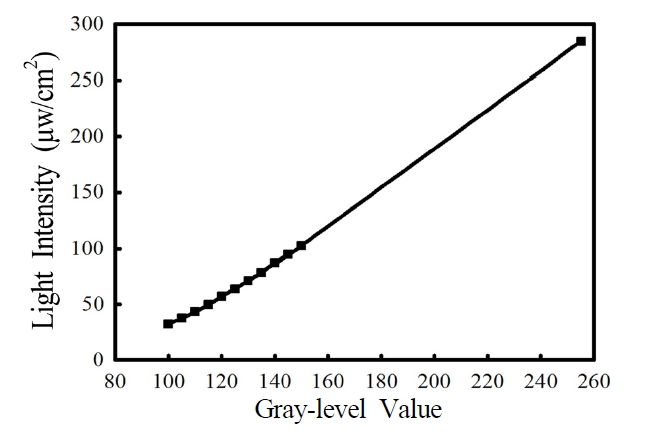
numerical aperture of 0.12 and reduces the software mask size in this system by 20x. A photodetector was used to measure the light intensity produced by the grayscale mask. Fig. 2 shows the variation of light intensity with the gray level value. The light intensity increases as the gray level value increases. To obtain a high-quality image for exposure, the DMD data were adjusted to a brightness of -33 and a contrast of +5. The proposed system does not require a physical mask and enables real-time monitoring of the exposure pattern on the PR. This facilitates modifying patterns, leading to relatively low development costs.
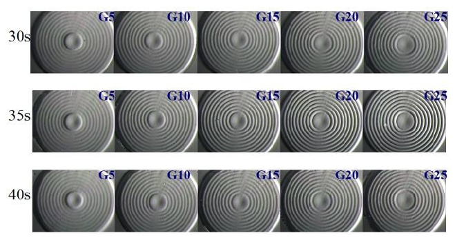
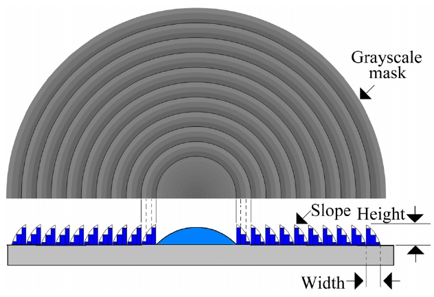
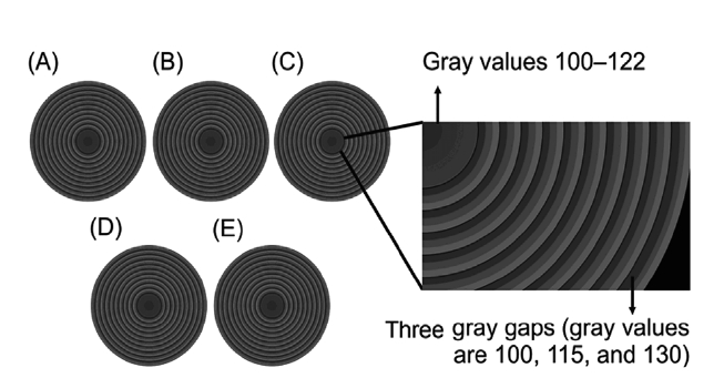
To facilitate the analysis, five masks with varying grayscale level rings were designed in this study, with each ring having the same width (Fig. 3). The grayscale level at the center of each mask ranged from 100 to 122. Each ring had three grayscale levels, starting at 100 and increasing in increments of 5, 10, 15, 20, or 25. Fig. 3(C) shows the mask with a grayscale level gradient of 15. The grayscale level gradient (G) represents different locations with varied gray levels, showing that grayscale data affect the forming characteristics that are used for large mask designs. In addition, the grayscale data can be used to adjust the mask size.
Microsoft PowerPoint was used to produce the mask pattern and playback mask because it can easily adjust the pattern size, as well as the grayscale value from 0 to 255. The experimental steps are as follows:; 1) clearing the wafer; 2) coating the PR on the wafer; 3) placing the wafer with the PR on the microscopy stage and moving it to the exposure area and focus position; 4) exposing the full screen mask; and 5) developing the PR after exposure.
3.1. Gray Level Value vs. Light Intensity
A DMD was used to produce images. Fig. 4 shows the gray gradient distribution, and Fig. 5 shows the gray level value relative to light intensity. As shown in Fig. 5, a high gray level value provides high light intensity. A high gray level value irradiation on positive PR, the result is a
short length, whereas a negative PR produces the opposite result.
3.2. Grayscale Gradient vs. Profile
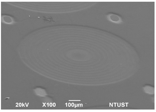
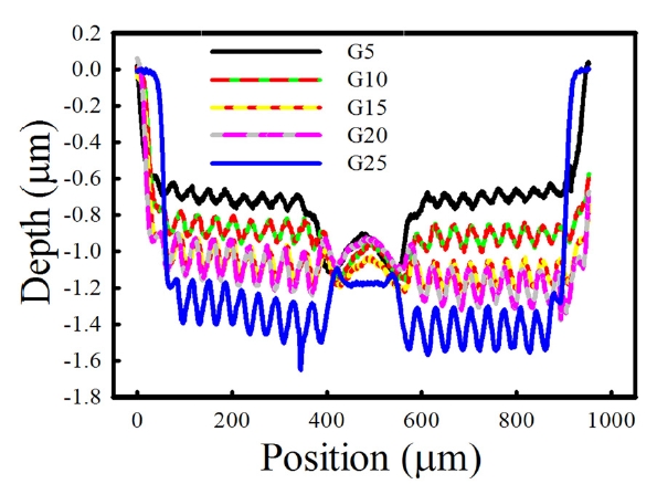
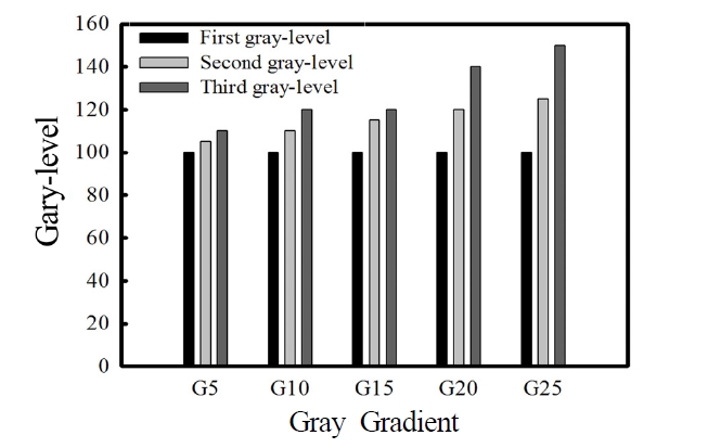
Figs. 6 and 7 show optical images and their corresponding scanning electron micrographs. A surface profilometer (Kosaka Laboratory, 3500DK) was used to measure the profile depth and width, with a resolution of 0 nm and a stylus tip radius of 2 μm. Fig. 8 shows the results, indicating that the depths of the central zones for masks with gray gradient 5(G5) and gray gradient 10(G10) are lower than those of the ring. This is because the maximal gray levels of the rings are 110 and 120, respectively, and the maximal gray level of the central zone is 122. Therefore, the light energy irradiation in the ring is lower than that in the central zone; thus, the central zone does not have the same depth as that of the ring.
For the mask with gray gradient 15(G15), the depth of the central zone is the same as that of the ring. This indicates that light irradiation in the central zone is consistent with that in the ring.
For the mask with gray gradient 20(G20), the depth of the ring is less than that of the central zone. The maximal gray level of the ring is 140, and that of the central zone
is 122. Finally, the central zone of the mask with gray gradient 25(G25) has the shallowest depth.
The ring mask used in this study has three grayscale levels, with energy increasing outward from the middle. The ring should form a right triangle. However, results indicate that the ring forms an acute triangle. This is likely because the ring of the maxima grayscale level producing the highest light energy that flows through the PR is reflected, affecting the initial grayscale level of the next ring. The ring subsequently forms an acute triangle and the depth is reduced, as inferred by examining the G20 and G25 masks.
Fig. 1 shows that the designed mask pattern should produce a right triangle. The G5 and G10 masks were compared for clarification. The first rings in both masks have a starting gray level of 100. The next gray levels are 105 and 110 for the mask with G5, and 110 and 120 for the mask with G10. However, the first ring in the mask with G5 is almost unformed, whereas the first ring of the mask with G10 is formed. The only difference between these two cases is the grayscale gradient. The maximal gray level in the center is 122, which is higher than the final gray level of the mask with G5(110), but close to the final gray level of the mask with G10. Although the designed
pattern should produce a right triangle, the design places a high-energy gray level close to a low-energy gray level. Thus, the high-energy light halo adds energy to the lowenergy gray level, resulting in the former affecting the latter. The object lens is not specialized for lithography applications because the depth of focus is short when the image focuses on the PR. Consequently, the mask image flowing through the PR is not vertical. The resulting reflection has a non-vertical reflection component. Thus, the final ring height is reduced. Fig. 9 shows this process.
For the mask with G15, the light energy irradiated in the central zone and that irradiated in the ring are the same. Therefore, the central zone and rings have the same depth.
3.3. Factors Affecting the Depth
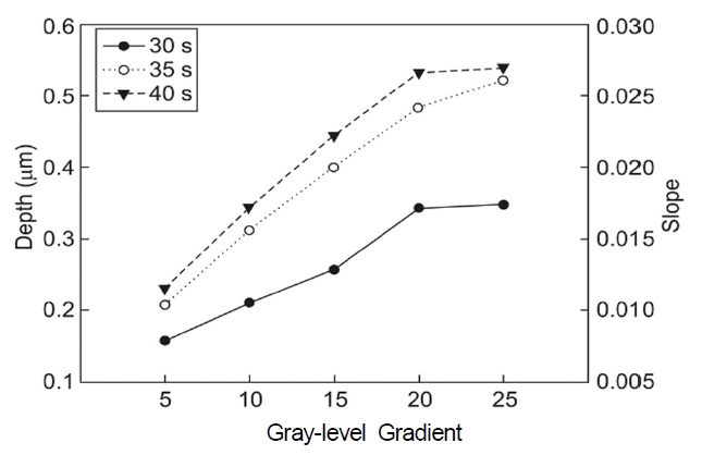
The slope factor is provided by the width and depth. In this study, every mask width is one size; therefore, changes in the width of the rings and changes in the gray level gradient and exposure time are slight. Fig. 10 shows the variations of depth and slope in the PR, depicting the gray level gradient at various exposure times. For each exposure
time, the increase in depth with an increase in the G(5 to 25) is 190 nm after 30 s of exposure, 313 nm for 35 s of exposure, and 307 nm for 40 s of exposure. Fig. 10 shows this trend. For the same gray level gradient, the results also show that the depth increases by 73-190 nm as the exposure time increases. There is a linear increase with a depth of up to G20, after which the depth appears to plateau. The energy then appears to achieve a critical value, and the PR exhibits nonlinear behavior.
3.4. Factors Affecting the Slope
Fig. 10 shows the variation of PR slopes with gray level gradients at various exposure times. For each exposure time, the slope of the PR increases with the gray level gradient. At a particular gray level gradient, the PR slope increases with longer exposure time. For example, at G5, the slope of the PR increases from 0.0084 to 0.0137 as the exposure time increases from 30 s to 40 s. When the exposure time is 35 s, the gray level gradient changes from 5 to 25. This produces the maximal PR slope of approximately 150%. These results indicate that the fabrication of a Fresnel zone lens using DMD maskless lithography should proceed as follows: First, the width of the mask should be fixed. Then, the grayscale gradient and values should be chosen based on the relative positions of the central zone and ring. If a smooth profile is required, more grayscale values and a smaller grayscale gradient should be used. Finally, the exposure time should be tested to achieve the correct profile.
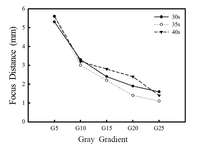
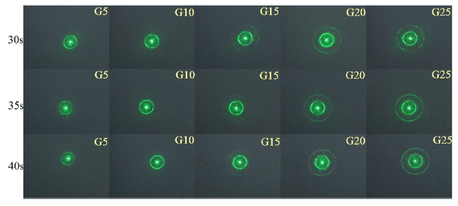
To test the final image result, we used a laser beam with a wavelength of 532 nm to irradiate a Fresnel lens pattern. Figs. 11 and 12 show the experimental design and image, respectively. The G5 image was smaller than all other images, demonstrating that G5 has a far focus, and the minimal length was achieved by G25 (Fig. 13). Under all conditions, the minimal distance was 1.1 mm, and the maximal distance was 5.6 mm.
This study presents a DMD maskless lithography system based on gray levels to fabricate Fresnel lenses with different ring slope designs. Maskless lithography involves using a simple and accurate design that can be used to produce various lens depths, ranging from 158 to 297 nm. The results indicate that the gray level gradient gap produces a small effect on the width of the rings. A greater gray level gradient signifies a greater depth and a larger slope of the ring design. The greatest depth achieved was 538 nm, and the maximal slope was 0.287. For the same exposure time, changes in the gray level gradient affected both the depth and slope. For G(5-25), the depth of the central zone was less than that of the ring. For G15, the depths of the central zone and ring were the same. When the central zone was higher than the ring, it caused the ring gray level to increase, which subsequently affected the profile and depth of the next ring. Using microscopy can provide a simple optical system, but the user must choose a specialized application in the lithography object lens to reduce the effect on adjacent areas by light that is not vertical. Optical test results show that differences between gray gradients have varying focus, with G5 having a far focus and G25 having a near focus. This result can serve as a reference for future design methods in 3D exposure technology.