Liquid crystal displays (LCDs) have been widely employed because they are thin, lightweight, and have low power consumption. With the recent increase in demand for highquality display devices, more attention has been given to the realization of an ultrahigh resolution system for the vivid display of images. However, since the decrease in pixel size for high-resolution LCDs gives rise to a small aperture ratio, very high transmittance is required.
Among the several available LC modes, the vertical alignment (VA) mode provides the best dark state, because the liquid crystal (LC) molecules are perfectly vertically aligned with the vertical alignment layer on the substrate [1]. However, LCs tilted downwards in one direction exhibit asymmetric viewing angle characteristics and a shift of the gamma curve [2-4]. To overcome this problem, several methods to realize a multi-domain structure have been proposed. The patterned electrodes and the protrusion structure make it possible to develop a multi-domain VA mode [5-7]. Although a multi-domain VA mode offers better viewing angle characteristics than a single-domain VA mode, the transmittance of a multi-domain structure decreases because of the presence of disclination lines at the domain boundaries. The micropatterned VA mode has been proposed to enhance the transmittance; however, the cross-shaped disclination lines formed by domain boundaries at the center of the pixel remain [8-9].
Recently, we have proposed a cross-shaped slit electrode structure to enhance the transmittance in a micro-patterned VA mode; in this method, the width of the disclination lines was reduced and the transmittance at the edges of each pixel was improved [10]. However, the width of the disclination lines at the center of the pixel must be further reduced.
In this paper, we propose a pixel electrode structure for high transmittance using the micro-patterned VA mode. We create a protrusion structure on the top substrate to reduce the width of the disclination lines at the domain boundaries. Using an optimized protrusion structure, the transmittance can be improved from 22.9% to 25.3%.
II. CONFIGURATIONS OF THE PROPOSED STRUCTURE
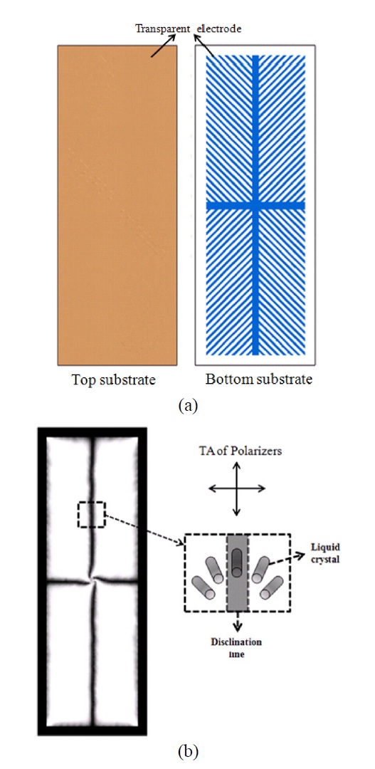
The top and bottom electrode structures of the micro -patterned VA mode are shown in Fig. 1 (a). A transparent electrode with no pattern is formed on the top substrate, whereas micro-patterned electrodes are formed on the bottom substrate. The micro-patterned VA mode exhibits a superior bright state under an applied voltage, as shown in Fig. 1 (b), because LCs are tilted downward, parallel to the micro-patterned electrodes. However, cross-shaped dis
clination lines limit the light throughput, resulting in a decrease in the transmittance. Disclination lines are caused by the continuous change of the LC alignment direction at domain boundaries, as shown in the inset in Fig. 1 (b).
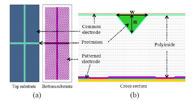
To create an abrupt change in the LC alignment direction, from -45° to +45°, at the domain boundaries, we created a protrusion structure on the common electrode of the top substrate, as shown in Fig. 2. The width of the protrusion is chosen to be the same as that of the cross-shaped electrode on the bottom substrate. The bottom electrode structure is the same as the conventional structure. Unlike the protrusion used in the conventional multi-domain VA mode, there is no light leakage in the proposed structure because the tilt direction of the LCs on the protrusion is coincident with the TA of the polarizers. Thus, there is no change in the dark state.
We employed commercial software, TechWiz LCD 3D (Sanayi System), to evaluate the proposed electrode structure. The parameters used for the numerical calculations are as follows. The dielectric and optical anisotropies of the LCs are -2.7 and 0.102, respectively. The thickness of the LC layer is 3.2 μm. The width of the micro-patterned electrodes, the gap between them, and the width of the cross-shaped backbone electrodes at the center of the bottom substrate are 2.3 μm, 2.7 μm, and 7 μm, respectively. The width, the height, and the dielectric constant of the protrusion structure are 7 μm, 1 μm, and 3, respectively. The length and width of each pixel are 300 μm and 100 μm, respectively.
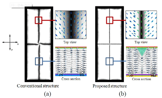
In the proposed structure, the width of the disclination lines is significantly reduced compared to the conventional structure, as shown in Fig. 3. Polar distribution of LCs in both of the conventional and proposed structures is almost the same as shown in the cross-sectional view because the electric field distribution is almost the same. In the top view, LCs in the conventional structure are continuously distributed between domains; therefore, disclination lines
are thick, because there are LCs whose azimuth angle is less than 45° relative to the TA of the polarizers. In the proposed structure, the protrusion structure dictates that LCs are distributed independently. Thus, it is easy for LCs near the center to follow the LCs aligned with the micro
micropatterned electrodes; thus, almost all of the LCs are aligned at 45° relative to the TA of the polarizers, resulting in high transmittance, because of the reduction in the disclination lines. The proposed protrusion structure allows an abrupt change in the alignment direction of LCs at the domain boundaries. Since the micro-slit in our previous work plays the role of the virtual protrusion, both of previous and proposed structures have almost the same mechanism of the tilt regulation at the region of cross-shaped electrode. Other than the region of cross-shaped electrode, the proposed structure shows the same distribution of LCs as previous structures [8,10].
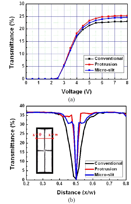
The calculated voltage-transmittance curves of the proposed structure and the conventional structure are shown in Fig. 4 (a). We also compared our results with that for the electrode structure that includes the previously proposed micro-slit at the position of the protrusion structure. [10]. All of the structures have the same saturation voltage of 8 V. The transmittances of the conventional, micro-slit, and proposed protrusion structures were 22.9%, 24.4%, and 25.3%, respectively. The highest transmittance was achieved when using the protrusion structure. To confirm the transmittance at the center of the pixel, we calculated the transmittance distribution, as shown in Fig. 4 (b). Herein, w is the pixel width. In the regions of x/w = 0.2 to 0.4 and 0.6 to 0.8 in both the conventional structure and the micro-slit structure, a transmittance of 37% was obtained. However, the proposed protrusion structure exhibits a transmittance of 37%, even in the regions of x/w = 0.2 to 0.48 and 0.52 to 0.8. Thus, we confirmed that the transmittance was enhanced to 25.3% when using the proposed protrusion structure. The transmittance can be increased from 25.3% to 28.2% when we use additional edge electrodes [10]. We also studied the dependence of the transmittance on the width and the height of the protrusion structure, as
shown in Table I. For a fixed height of 1 μm, the highest transmittance was obtained when the width of the protrusion was the same as that of the cross-shaped electrode on the bottom substrate. When the width of the protrusion was 7 μ m, the highest transmittance was shown at a height of 1 μ m. When the height of the protrusion is too low, isolation effect by the protrusion is weak. When the height of the protrusion is too high, the polar angle of LCs is large so that the transmittance becomes low. In all cases, however, we can obtain a higher transmittance than when using the conventional structure. In addition, choice of the protrusion material might be an important parameter.
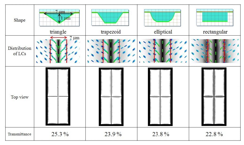
Under the optimal condition, we considered several protrusion shapes, such as a triangle, trapezoid, ellipse, and rectangle, as shown in Fig. 5. In all structures, the alignment direction of the LCs showed an abrupt change at the center of the protrusion structure; thus, the width of the disclination lines was reduced. Among them, the triangular structure showed an enhancement of transmittance of 25.3%. Although other structures also exhibited a higher transmittance than that of the conventional structure, grayish disclination lines near the cross-shaped electrode were observed in the top images of the bright state, because the azimuth angle of the LCs at the protrusion boundary was less than 45° relative to the TA of the polarizers. Irrespective of the shape of protrusion, there is no light leakage in the dark state because LCs are aligned parallel to the TA of polarizers.
In conclusion, we proposed a multi-domain VA LCD that achieves high transmittance. We created a protrusion on the top substrate so as to reduce the width of the disclination lines at the domain boundaries. We expect that the proposed method can contribute to the realization of high-resolution LCDs.