검색 전체 메뉴
PDF
맨 위로
OA 학술지
Optical Proximity Corrections for Digital Micromirror Device-based Maskless Lithography
  • 비영리 CC BY-NC
  • 비영리 CC BY-NC
ABSTRACT
Optical Proximity Corrections for Digital Micromirror Device-based Maskless Lithography
KEYWORD
Digital micromirror device , Maskless lithography , Optical proximity correction , Edge placement error , Corner-rounding effect
  • I. INTRODUCTION

    In conventional photolithography using a photomask, various optical proximity corrections (OPCs) have been used to compensate for imaging errors such as edge placement and corner-rounding errors in order to achieve desired features in a pattern [1-9]. However, the use of a photomask is expensive and increases turnaround time. Maskless lithography involves the use of a digital micromirror device (DMD) as a virtual mask in place of a physical mask; this alternative method requires only binary data for the modulation of the light [10-16].

    Nevertheless, a different method is required to utilize conventional OPCs in maskless lithography. OPCs in conventional photolithography generally target image errors in nanoscale patterns caused by diffraction and employ the mask shapes to compensate for these image errors [17, 18]. On the other hand, in DMD-based maskless lithography, OPCs target image distortions in each microscale beam projected by mirror devices and the dose distribution produced by an accumulation of projected beam images [19, 20]. This difference is the reason that our study focuses on controlling the modulation of the spatial light by using micromirrors in order to achieve desired features in a microscale pattern.

    In this work, optical proximity corrections (OPCs) for DMD-based maskless lithography are proposed to compensate for the edge placement error (EPE) and the corner-rounding effect by a simulation and experimental approach, respectively. A model is derived for obtaining the dose distribution profile from the projected beams of micromirrors and for obtaining their resulting structure in the fabrication of a photoresist by analyzing the pattern writing scheme of a DMD-based maskless lithography system. Pre-compensation is numerically applied to the design intent prior to fabrication, which is obtained based on the model, reducing EPE. Moreover, by adding an assistant serif to the corners of a feature, referred to as the conventional optical proximity correction (OPC) method, and controlling light transmission by modulating a DMD, the corner-rounding effect is experimentally minimized. Redundancy, a new parameter defined as the number of writing times is derived from analyzing the pattern writing scheme of a DMD-based maskless lithography system, and applied to controlling light transmission. Compared to the traditional works [19, 20] which present only a feasibility study by a numerical simulation, the proposed method is based on a substrate scanning manner encouraging an attempt to a mass production, and the experiment using the industrial DMD-based maskless system confirms that this method is promising for minimizing a corner-rounding effect.

    II. DMD-BASED MASKLESS LITHOGRAPHY SYSTEM

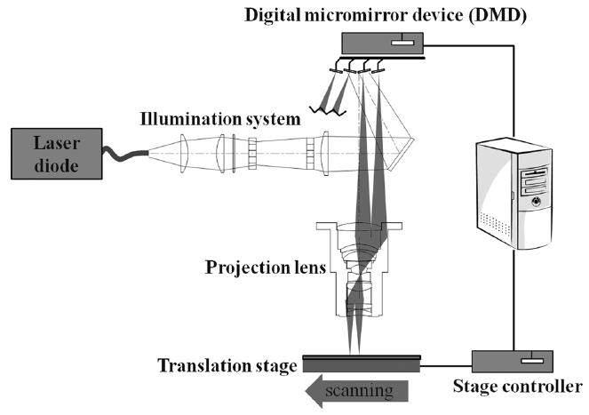
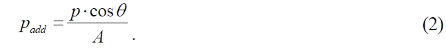
    A schematic for DMD-based maskless lithography is shown in Figure 1. In the system for our experiments, UV light with a central wavelength of 405 ± 2 nm is delivered from a laser diode system (EPICO Co., Ltd.) with an optical power of 2.2 W along the optical fiber. An illuminating system (POMT Co.) with a maximum chief ray angle of 11.0°, containing a fly-eye and condenser lens, achieves a light uniformity of over 97% on the surface of a micromirror array. A Texas Instruments DMDTM with a 1024 × 768 array of 13.68 μm wide micromirrors is used as a light modulator instead of a photomask. The individual micromirrors selectively reflect UV light collected by the illumination system towards the projection lens. A 1.8 × projection lens (POMT Co.) with an objective numerical aperture of 0.1 produces an aerial image of the micromirrors with a size of 25 μm each on the surface of the photoresistcoated substrate; this aerial image is shown in Figure 2.

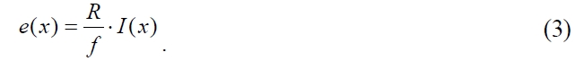
    For each beam, the intensity does not have a box profile with a sharp edge but rather a flat top decay edge, i.e., with a flat top and with edges decreasing to form rounded corners. The beam profile is difficult to quantify and is often variable on a case-by-case basis, depending on the setup and system component performance. For this reason, the beam

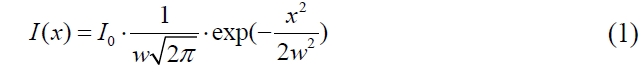
    profile on the photoresist surface is generally assumed to be a light spot [21, 22], which is applied to the simulation for compensating EPE.; hence, the intensity can be expressed as a Gaussian distribution using the first-order approximation of the point spread function [23]:

    image

    where I0 is the peak intensity and w is the Gaussian radius.

    III. PROCESS MODEL FOR OBTAINING THE PROFILE OF PHOTORESIST STRUCTURE

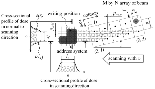
    The M × N array of a beam produced by a DMD is imaged onto the surface of the photoresist. The feature contour of the desired pattern is required to be filled by overlay writing using the beams from the DMD. Improvement of the address resolution by setting a high writing density can enhance the lithographic resolution. In order to make this resolution improvement possible, a photoresist-coated substrate is scanned with a constant velocity (v), and the DMD is simultaneously installed in order to tilt the array of the projected beams at a specific angle in the scan direction. For the array consisting of 2 × 5 beam elements, shown in Figure 3, the beam array is installed at a tilting angle (θ) of arctan(1/4) with respect to the scanning direction. For the general arrangement of M×N elements, the DMD is tilted at a specific angle in order to align the beam elements (i, j) and (i+1, j+A) along a common line parallel to the scan direction of the substrate; here, A is an integer defined as the writing period. A is 4 in the example shown in Figure 3. Using this configuration, two address lines, which are scanning paths of the beam elements to (1, 1) and (2, 1), adjacently placed along the row direction, can be separated into four sectors by the

    address lines of the three beam elements to (2, 2), (2, 3), and (2, 4). Therefore, the minimal distance between each address line on the surface of the photoresist, defined as the address pitch (padd) along the direction perpendicular to the scanning direction, can be made smaller than the beam pitch (p):

    image

    The moving pitch (pmov) is defined as the distance scanned by the substrate during the time taken by the mirrors to switch their state. Setting pmov equal to padd fixes the pitch of the address system, along both the direction perpendicular to the scanning direction and the scanning direction, as padd. Therefore, for writing on the surface of photoresist, an address system with a significantly smaller pitch address than that of p is constructed. Here, pmov is expressed as v /f, where f is the frequency of the DMD to switch its state.

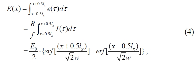
    In this address system, the writing position within the contour of the desired feature, shown in Figure 3, is repeatedly written by periodic beam elements, placed at the writing period (A) along the column direction and placed at one period along the row direction. In this system, with a beam array of 1024 × 768 elements, the writing position is written 192 times by mirror elements to (1, 1), (2, 5) through (192, 765), yielding the dose profile [e(x)]. The number of times one position is written is defined as redundancy (R), where R = N/A with an M × N beam array tilted at θ < 45°. Therefore, the dose profile produced by multiple beam writing at one position is

    image

    Redundancy is a key parameter to control light transmission to parts of a feature, and it is determined to be an experimental variable for compensating the corner-rounding effect. Because in a DMD-based maskless lithography system the light transmission is determined by the number of writing times at one position, even though in conventional photolithography it was achieved using gray photomasks.

    As shown in the cross-sectional profile at normal to the scanning direction in Figure 3, doses [e(x)] are written on positions along a line width (lx) of the desired feature with a period of padd. By setting A to large values and thus reducing the pitch of the address system, padd, the accumulated dose profile [E(x)] of all doses over a given line width (lx) can be approximated as terms of the Gaussian error function

    image

    where lx is the desired width of a feature and E0 is the saturation dose for the larger values of feature width. In the same manner, by setting f to large values and thus reducing the pitch of the address system, pmov, the accumulated dose profile [E(y)] can also be obtained.

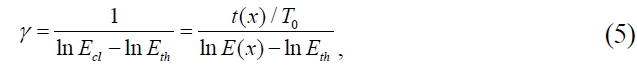
    In general, the profile of photoresist material, for either positive or negative development processes, can be expressed as a function of dose transferred to a photoresist [24]. For a positive photoresist, the threshold dose (Eth) is defined as the minimum exposure dose required to trigger a photoresist reaction. The photoresist is completely removed when the dose reaches the clearing dose (Ecl). From these doses, the contrast (γ) characterizing a photoresist is defined as

    image

    where t(x) is the final photoresist profile, 0 ?t(x) ≤T0, EthE(x) ≤Ecl, and T0 is the thickness of the photoresist. The resultant profile of the photoresist, with a variable feature width, is then obtained from Eq. (5):

    image

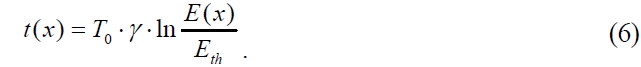
    Strictly the precise profile of the photoresist may not be obtained from Eq. (6). Since the resist model given by equation (6) makes the simple assumption that all resist development occurs vertically. This is not the case, because development proceeds vertically in a clear region, then changes to a horizontal development as it approaches the feature edge. Nevertheless the significance of this work is on the procedure of OPC for a DMD-based maskless system rather than on the accuracy of predictions.

    IV. RESULT OF SIMULATION AND EXPERIMENT

       4.1. Edge Placement Error Correction

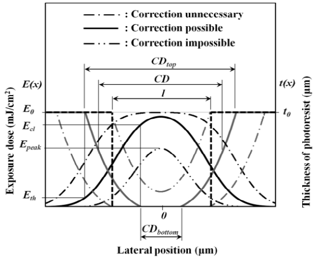
    The critical dimension (CD) of the resultant photoresist is assumed to have an average value of CDtop and CDbottom, defined as the width dimensions on the top (100% height) and bottom (0% height) of the photoresist profile respectively as shown in Figure 4, and calculated from Eq. (6). In principle, a CD for the photoresist profile equal to the design width can be achieved by properly setting the saturation dose (E0). However, this assumption is only approximate in practice. The normalized depth of remaining photoresist, plotted in Figure 5, is expressed by the normalized peak dose from Eq. (4):

    image

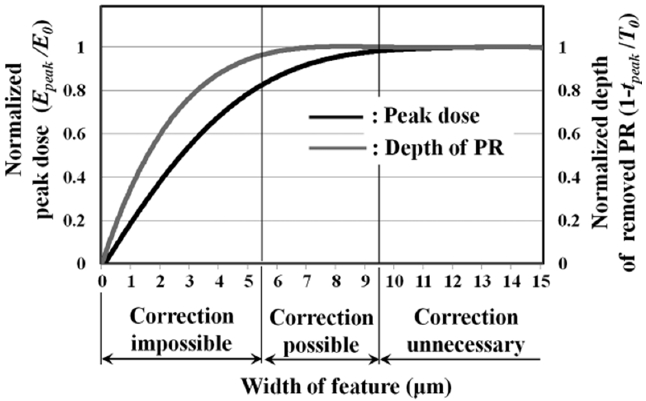
    The normalized peak dose and depth of the removed photoresist become saturated with increasing design width. In this condition, the CD of the resultant photoresist profile is equal to the desired width, rendering any correction unnecessary. However, with decreasing design width, the normalized peak depth becomes smaller than unity, which

    implies that a photoresist structure with CD equal to the design width is not possible. This displacement error can be corrected using either width or dose pre-compensation, that is, by increasing the design width or the saturation dose in advance, respectively. Nevertheless, there are limitations to pre-compensation corrections. For instance, either the range of design widths leading to a structure has a very small peak depth to reach the surface of the substrate or the CD does not reach the desired design width.

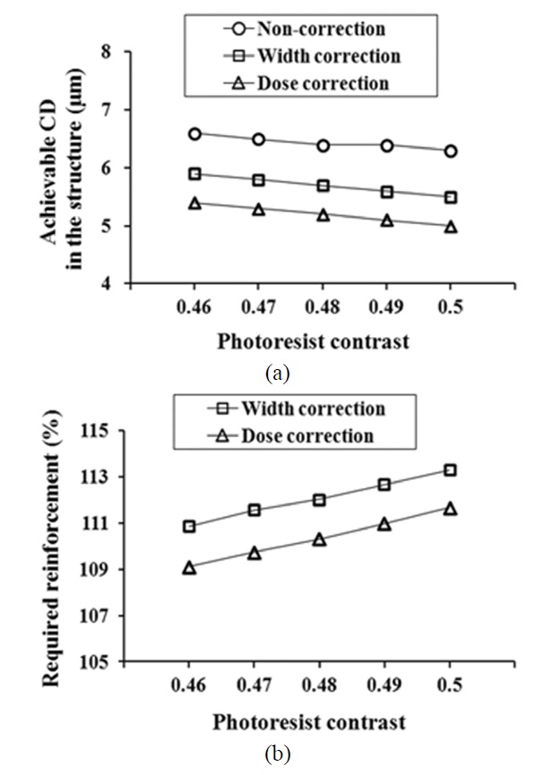
    Simulations for reducing the EPE of a feature within the range of possible corrections are conducted under the following conditions. The contrast (γ), normalized threshold dose (Eth/E0), thickness (T0) of the photoresist, and the Gaussian radius (w) of the point beam are 0.46, 0.1, 1 μm, and 2 μm respectively. To quantify correction performance for the design width of a feature, we introduce the matching index (%), defined as l/CD × 100. Figure 6 shows a plot of the matching index and the reinforcement required for adjusting the CD versus the design width. The width and dose corrections shown in Figure 6 are those needed to adjust the matching index to 100%. The matching index curve indicates the data without the width and dose corrections. We find that the matching index decreases from 107.8% to 0% as the width increases from 6.6 μm to 9.5 μm. For width less than 6.6 μm, an unacceptable photoresist is fabricated, which is not completely removed from the surface of the substrate during the development. Without corrections, the minimum achievable CD for the photoresist structure is 6.6 μm. Moreover, a resultant structure with a width of over 9.5 μm no longer needs correction. If this feature is previously compensated by a width reinforcement of 110.9%, the feature can be corrected with a matching index of 100% and the obtainable CD can be reduced to 5.9 μm. The achievable CD can be reduced to 5.4 μm using a dose reinforcement of 109.1%. This result shows that using width and dose compensation, the lithographic resolution can be, respectively, enhanced to 11.8% and 22.2% more than that for the case in which no correction is made.

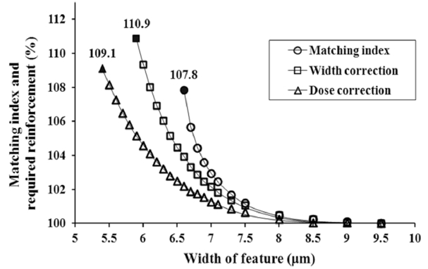
    In Figure 7(a), the plot of the achievable CD of the resultant photoresist structure versus contrast is shown for the cases without any correction, with width correction, and with dose correction. Further, the plot of the required width and dose reinforcements versus contrast is shown in Figure 7(b). The achievable CD decreases with increasing photoresist contrast, thereby realizing a high lithographic resolution. Further, less reinforcement is required for dose correction as compared to that for width correction.

       4.2. Corner Rounding Correction

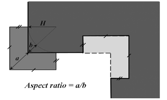
    As in conventional lithography using a photomask, corners of a sharp design feature (Figure 8(a)) are rounded in resultant structures in maskless lithography, as shown in Figure 8(b). Conventional OPC methods are rule based [5, 6] or model based [7, 8] for the pre-compensation of design features and are useful references for correcting corner-rounding in DMD-based maskless lithography. In the present work, we added an assistant serif with a square shape to the corner of the feature and modulated the dose at this serif for minimizing corner-rounding.

    For experiments, p and A are set to 25 μm and 16, respectively, yielding a padd of 1.5 μm. The v and f are set to 24 mm/s and 15,400 Hz, respectively, yielding a pmov of 1.5 μm. A positive photoresist (AZ1512®, Clariant Corporation) was used for the fabrication of a feature; this photoresist was spin-coated on a silicon substrate and had a thickness of 1.2 μm.

    4.2.1. Adding Assistant Serif

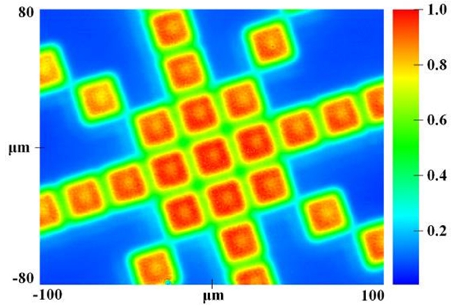
    The assistant serif was expected to increase the dose at the convex corners and decrease it at concave corners, as shown in Figure 9. We assume that the geometry of the serif is defined by two factors: the serif length (H) and the aspect ratio defined by a/b. Fabrications with different serifs were conducted, the resultant structure of the photoresist was evaluated in each case, and finally, the best serif for the compensation was determined. Pre-compensation for corner rounding is evaluated using the matching rate [Eq. (8)], which, in turn, is calculated from a pixel-wise operation between two images: the design image, D [Figure 8(a)],

    and the binarization image, B [Figure 8(c)]. B is obtained from the resulting image [Figure 8(b)]:

    image

    where Di,j and Bi,j are the binary depths at the pixel positions of (i, j) for D and B, respectively.

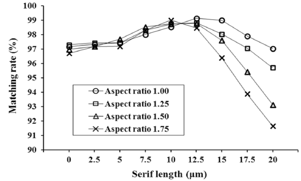
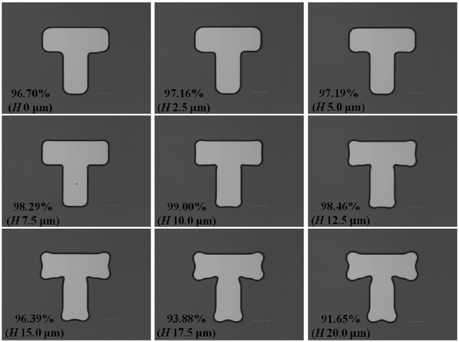
    The matching rate for a T-shape feature [Figure 8(a)] along the serif length with a difference aspect ratio is shown in Figure 10. The maximum matching rate is 99.14% with a serif length of 12.5 μm and an aspect ratio of 1.00. Matching rates of 98.82%, 98.76%, and 99.00% were found with aspect ratios of 1.25, 1.5, and 1.75, respectively, and serif lengths of 12.5, 12.5, and 10.0 μm, respectively. It was found that the matching rate gradually increased with increasing serif length and sharply decreased above a maximum matching rate. For the serif with an aspect ratio of 1.75, the resulting images with increasing serif length are shown in Figure 11. The matching rate for features with a serif length (H) of 0 μm is 96.7%, fabricated without pre-compensation.

    With increasing serif length, the matching rate increases and the rounding of the corner gradually disappears. In this way, the image of the resultant feature is more similar to the design [Figure 8(a)]. Finally, at a serif length of 10.0 μm, the matching rate becomes 99.00% and the shape of the resultant feature is most similar to that of the design feature. Further increase in the serif length results in a sharp decrease in the matching rate, owing to the side effects of excessive pre-compensation.

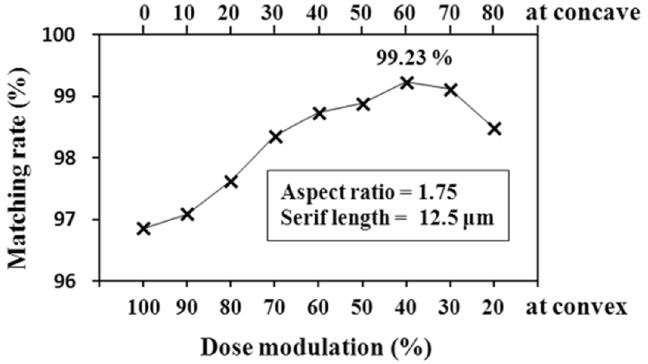
    4.2.2. Modulating Dose onto the Serif

    In conventional photolithography, an OPC method has been used to control light transmission to parts of a feature using gray photomasks [9]. For maskless photolithography, dose modulation is proposed as a digital correction method. As described previously, DMD-based maskless lithography involves writing a beam R times at a single writing position. By controlling R within the contour of the assistant serif in a feature, dose modulation can be achieved. In a previous experiment, we concluded that the best pre-compensation for the T-shape feature with an aspect ratio of 1.75 is achieved at a serif length of 10.0 μm. Only a decrease or increase in dose can be used to modulate the serif at a convex or concave corner, respectively. Thus, for a serif of 12.5 μm length, which can permit excess compensation, the resultant photoresist is fabricated with a decreasing dose at the convex corner and an increasing dose at the concave corner. As shown in Figure 12, a feature pre-compensated by a dose modulation of 40% and 60% at the convex and concave corners of a serif, respectively, achieves a 99.23% matching rate and is, thus, most similar to the desired design feature.

    V. DISCUSSION

    Two approaches were used for resolution enhancement, to correct the EPE and corner-rounding error. For simulation of the lithography process to reducing the EPE, we used a dose and structure model, which was derived by approximating the intensity of the beam to the Gaussian distribution, as was done in previous studies. In spite of the approximation, our confirmation that the EPE can be reduced to enable improvement of the CD is reasonable, because the beam intensity distribution decays exponentially. The reduction of corner-rounding was achieved experimentally.

    VI. CONCLUSION

    We derived a theoretical model for obtaining the dose distribution using DMD-based modulation on the surface of a photoresist and for obtaining the resulting profile of the fabricated photoresist structure. Using model simulations, we confirmed that EPE corrections are classified into three categories: those where correction is unnecessary, those where correction is possible, and those where correction is not helpful in achieving the design width. In the case where corrections were possible, the EPE was clearly reduced using pre-compensation of either the design width or the dose. This pre-compensation of the design width and dose improved the lithographic resolution from 6.6 μm to 5.9 μm and 5.4 μm, respectively. For minimizing corner-rounding, an assistant serif was added to the corners of a feature and the light transmission was controlled by modulating a DMD as a digital correction, thereby improving the shape matching rate between a resultant feature and the desired design from 96.7% to 99.23%.

    In this paper, we focused on enhancing an isolated feature in a lithographic pattern. The spatial spread of intensity causes overlap between neighboring features owing to imperfections in the optical imaging system. In turn, this overlap leads to an additional shift in edge placement and corner deformation in the resultant photoresist. Resolution enhancements for closely spaced features will be investigated in a future study.

참고문헌
  • 1. Wong A. K. 2001 Resolution Enhancement Techniques in Optical Lithography google
  • 2. Chen J. F., Laidig T., Wampler K. E., Caldwell R. (1997) “Optical proximity correction for intermediate-pitch features using sub-resolution scattering bars” [J. Vac. Sci. Technol. B] Vol.15 P.2426-2433 google
  • 3. Zhang H., Morrow J., Schellenberg F. M. (1998) “Optical proximity correction: a detail comparison of techniques and their effectiveness” [Microelec. Eng.] Vol.41-42 P.79-82 google
  • 4. Li Y., Yu S. M., Li Y. L. (2009) “Intelligent optical proximity correction using genetic algorithm with model- and rule-based approaches” [Comput. Mater. Sci.] Vol.45 P.65-76 google
  • 5. Otto O. W., Garofalo J. G., Low K. K., Yuan C. M., Henderson R. C., Pierrat C., Kostelak K. L., Vaidya S., Vasudev P. K. (1994) “Automated optical proximity correction: a rules-based approach” [Proc. SPIE] Vol.2197 P.278-293 google
  • 6. Park J.-S., Park C.-H., Rhie S.-U., Kim Y.-H., Yoo M.-H., Kong J.-T., Kim H.-W., Yoo S.-I. (2000) “An efficient rule-based OPC approach using a DRC tool for 0.18 μm” [ASIC Proc. IEEE] Vol.2000 P.81-85 google
  • 7. Levenson M. D., Viswanathan N. S., Simpson R. A. (1982) “Improving resolution in photolithography with a phase-shifting mask” [IEEE Trans. Electr. Dev.] Vol.29 P.1828-1836 google
  • 8. Liu Y., Zakhor A., Zuniga M. (1996) “Computer aided design of phase shift mask designs with reduced complexity” [IEEE Trans. Semiconductor Manufacturing] Vol.9 P.170-181 google
  • 9. Cui Z., Dua J., Huanga Q., Sua J., Guoa Y. (2000) “Optical proximity correction by grey tone photolithography” [Microelec. Eng.] Vol.53 P.153-156 google
  • 10. Shirota H., Kuwabara A. (2005) “Pattern writing apparatus and pattern writing method” google
  • 11. Ljungblad U. B., Askebjer P., Karlin T., Sandstrom T., Sjoeberg H. (2005) “A high-end mask writer using a spatial light modulator” [Proc. SPIE] Vol.5721 P.43-52 google
  • 12. Okuyama T., Washiyama H. (2006) “Multi-exposure drawing method and apparatus therefor” google
  • 13. Seo M., Kim H. (2007) “Lithography upon micromirrors” [Computer-Aided Design] Vol.39 P.202-217 google
  • 14. Liang J., Kohn Jr. R. N., Becker M. F., Heinzen D. J. (2010) “High-precision laser beam shaping using a binary-amplitude spatial light modulator” [Appl. Opt.] Vol.49 P.1323-1330 google
  • 15. LEE D.-H. (2010) “Optical system with 4 μm resolution for maskless lithography using digital micromirror device” [J. Opt. Soc. Korea] Vol.14 P.266-276 google
  • 16. Huang Y.-H., Jeng J.-Y. (2012) “Forming a fresnel zone lens: effects of photoresist on digital-micromirror-device maskless lithography with grayscale exposure” [J. Opt. Soc. Korea] Vol.16 P.127-132 google
  • 17. Pati Y. C., Kailath T. (1994) “Phase-shifting masks for microlithography: automated design and mask requirements” [J. Opt. Soc. Am. A] Vol.11 P.2438-2452 google
  • 18. Khoh A., Samudra G. S., Wu Y., Milster T., Choi B.-I. (2004) “Image formation by use of the geometrical theory of diffraction” [J. Opt. Soc. Am. A] Vol.21 P.959-967 google
  • 19. Guo X., Dub J., Luo X., Deng Q., Duc C. (2008) “RET simulations for SLM-based maskless lithography” [Microelec. Eng.] Vol.85 P.929-933 google
  • 20. Kessels M. V., Heggarty K. (2009) “Optical proximity correction for a versatile LCD based direct write maskless photoplotter” [Microelec. Eng.] Vol.86 P.2385-2391 google
  • 21. Sun C., Fang N., Wu D. M., Zhang X. (2005) “Projection microstereolithography using digital micro-mirror dynamic mask” [Sens. Actuators A: Physical] Vol.121 P.113-120 google
  • 22. Meisburger W. D. (2009) “Apparatus for SLM-based optical lithography with gray level capability” google
  • 23. Kumar G. R. V., Sayanagi K. (1968) “Measurement of optical transfer function by its moments” [J. Opt. Soc. Am.] Vol.58 P.1369-1376 google
  • 24. Sheats J. R., Smith B. W. 1998 Microlithography: Science and Technology google
OAK XML 통계
이미지 / 테이블
  • [ FIG. 1. ]  Schematic of DMD-based maskless lithography system.
    Schematic of DMD-based maskless lithography system.
  • [ FIG. 2. ]  Aerial image of the micromirrors on the surface of a photoresist.
    Aerial image of the micromirrors on the surface of a photoresist.
  • [ FIG. 3. ]  The principles of operation of the DMD-based maskless system and the production of accumulated dose. θ is the tilting angle of the beam array, p is the beam pitch, w is the Gaussian radius of the beam spot, v is the scanning velocity of a substrate, padd is the address pitch of the address system, pmov is the moving pitch by a substrate, e(x) is the dose profile produced by multiple beam writing, E(x) is the accumulated dose over a given line width, and lx and ly are the line widths of the desired feature.
    The principles of operation of the DMD-based maskless system and the production of accumulated dose. θ is the tilting angle of the beam array, p is the beam pitch, w is the Gaussian radius of the beam spot, v is the scanning velocity of a substrate, padd is the address pitch of the address system, pmov is the moving pitch by a substrate, e(x) is the dose profile produced by multiple beam writing, E(x) is the accumulated dose over a given line width, and lx and ly are the line widths of the desired feature.
  • [ FIG. 4. ]  Accumulated dose and resultant photoresist profile. l is the design width of the feature. CDtop and CDbottom are the width dimensions at the top and bottom, respectively, of a photoresist. CD is assumed to be (CDtop+CDbottom)/2. The long-dash dotted lines, solid lines, and long-dash double-dotted lines are the profile of the accumulated dose (black) and resultant photoresist (gray) when the corrections are unnecessary, possible, and impossible, respectively.
    Accumulated dose and resultant photoresist profile. l is the design width of the feature. CDtop and CDbottom are the width dimensions at the top and bottom, respectively, of a photoresist. CD is assumed to be (CDtop+CDbottom)/2. The long-dash dotted lines, solid lines, and long-dash double-dotted lines are the profile of the accumulated dose (black) and resultant photoresist (gray) when the corrections are unnecessary, possible, and impossible, respectively.
  • [ FIG. 5. ]  The variation of normalized peak dose (black), and normalized depth (gray) of a removed photoresist along the width of the feature.
    The variation of normalized peak dose (black), and normalized depth (gray) of a removed photoresist along the width of the feature.
  • [ FIG. 6. ]  Matching index versus design width and the required reinforcement of width and dose in order to correct to 100% of the matching index.
    Matching index versus design width and the required reinforcement of width and dose in order to correct to 100% of the matching index.
  • [ FIG. 7. ]  (a) The achievable CD of a resultant structure and (b) the required reinforcement of width and dose with the variable contrast of a photoresist.
    (a) The achievable CD of a resultant structure and (b) the required reinforcement of width and dose with the variable contrast of a photoresist.
  • [ FIG. 8. ]  Images of a T-shape feature. (a) Design image (D), (b) resulting image (R), and (c) binarization image (B).
    Images of a T-shape feature. (a) Design image (D), (b) resulting image (R), and (c) binarization image (B).
  • [ FIG. 9. ]  Pre-compensation by adding a serif, defined by the serif length (H) and aspect ratio (a/b), to the corner of a feature.
    Pre-compensation by adding a serif, defined by the serif length (H) and aspect ratio (a/b), to the corner of a feature.
  • [ FIG. 10. ]  Matching rate with difference serif of T-shape features.
    Matching rate with difference serif of T-shape features.
  • [ FIG. 11. ]  Images and matching rate of T-shape feature with an aspect ratio of 1.75.
    Images and matching rate of T-shape feature with an aspect ratio of 1.75.
  • [ FIG. 12. ]  Matching rate with difference dose modulations at assistant serifs of the feature.
    Matching rate with difference dose modulations at assistant serifs of the feature.
(우)06579 서울시 서초구 반포대로 201(반포동)
Tel. 02-537-6389 | Fax. 02-590-0571 | 문의 : oak2014@korea.kr
Copyright(c) National Library of Korea. All rights reserved.