Optical switches are essential components in high speed optical communication systems and networks. Implementation of optical switches based on the silicon on insulator (SOI) has attracted many researchers in recent years [1-4]. SOI substrates are intrinsically compatible with CMOS electronics, allowing access to a mature manufacturing infrastructure and the ability to combine photonic and electronic networks on a single chip [5]. The centrosymmetric crystal structure of silicon prohibits native silicon from possessing the Pockels effect, with the result that switches tend to be either very long or require high powers to operate. This problem limits the use of silicon in photonic integrated circuits (PICs) [6]. The thermo-optic effect in silicon is comparatively higher than EO effect, but the switching time above 1 μs is an important limitation in thermo-optic devices [2, 8].
Slow light (SL) can reduce the power or the physical length of the switch by enhancing the lightwave-matter interaction [7, 9-11]. In the slow light regime, the optical signal is compressed and hence the pulse amplitude is increased, which causes the enhancement of the linear and nonlinear effects in the structure. Linear effects such as gain, thermo-optic and electro-optic are scaled with the slowdown factor, whereas the nonlinear effects scale with its square [12, 13].
Photonic crystals (PCs) can be engineered to create new functionalities such as variation of the dispersion diagram to slow down the speed of light [1, 7, 9 and 10]. It is possible to design slow-light photonic crystal structures to attain high slow down factor and low group velocity dispersion (GVD) through engineering the geometry of the photonic crystal structure [9, 10, 14, 15]. Injecting the electro-optic (E-O) or nonlinear materials to the slot region of the slotted PCW results in slow down and confinement of the light and tuneability of the devices [5, 16, 17, and 19]. Nevertheless, the in-slot E-O efficiency is relatively low (~10% - 30%) compared with the value of bulk E-O polymer [20, 28]. Recent research has shown that large leakage current during the poling process can degrade the poling efficiency and E-O coefficient [18]. Using new E-O polymer materials (such as 15% wt. AJLZ53/polymethyl methacrylate) [20, 21] with lower conductivity in a wide slot will significantly reduce the leakage current, and it can increase the thin film poling efficiency [21, 22]. Recently, effective in-device E-O coefficient of 735 pm/V on electro-optic polymer infiltrated silicon photonic crystal slot waveguides has been demonstrated [21].
Another common problem in silicon photonic devices is the temperature dependence of the optical properties due to the thermo-optic effect of silicon [21]. Although the thermal expansion effect has been considered in some research on optical sensors [38] but variation of the silicon refractive index with temperature has not been taken into account in the previous research on PC switches and modulators, whereas it has a considerable effect on the optical properties of the devices. As an example a 38℃ temperature variation corresponds to variation of 6.8×10⁻³ in refractive index which is enough to perform switching in some PC switches [24, 25]. Hence, reduction of the temperature sensitivity of the device is necessary [1, 26].
We present a solution to improve the E-O performance in SOI by means of polymer infiltrated SPCDC to design a slow light photonic crystal switch. As the polymers offer very high Pockels coefficients [5], infiltration of the SPCDC by polymer enhances the E-O effect in the designed structure and causes switching in the very short length. Proper E-O material with low conductivity in a wide slot will sufficiently increase the poling efficiency and enhances in-device E-O coefficient [21, 28, and 29]. However, the thermal dependence of silicon’s and polymer’s refractive indexes are typically of different sign. So opposing the thermo-optic effect of the polymer can minimize or even eliminate the temperature dependence of the device for a given operating point [27, 30]. We have shown that the designed structure is stable for temperature variation of
This paper is organized as follows. The design of the slow light slotted PC directional coupler will be discussed in the next Section. The switch is designed and its performance and thermal stability are demonstrated in Sections 3 and 4, respectively. The paper is concluded in Section 5.
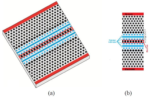
The planar slotted photonic crystal directional coupler can be implemented by replacing two rows of air holes in the triangular lattice PC with narrow slots, as displayed in FIG. 1. Two slotted photonic crystal waveguides (SPCW) are placed sufficiently close that the optical modes in each waveguide overlap and interact with each other. As for the conventional directional coupler, odd and even supermodes are supported in this structure [1]. Each mode has a different wavevector and therefore light in the system will couple from one waveguide to the other after encurring a relative phase difference of
dispersion engineering is necessary to shorten the switching length [1, 2].
Since the innermost rows of the holes in SPCW have the most important impact on the dispersion diagram [1, 15, 31], these rows are modified for engineering the dispersion diagram of the odd and even modes. The slot and the innermost rows in each SPCW are infiltrated with polymer, as illustrated in FIG. 1b. The structure is considered to have the geometry parameters of silicon refractive index of
To increase the polling efficiency and enhance the effective E-O coefficient (r33), it is necessary to use a wide slot [21, 28]. Although the effective in-device r33 of 735 pm/V from an electro-optic polymer infiltrated slotted silicon photonic crystal waveguide with the slot width of W= 0.75
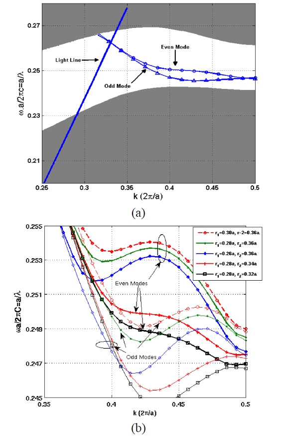
Figure 2(a) shows the odd and even supermodes in the band gap. The flat band part of the even mode and operation point of the switch is below the light line and it means a good light confinement in the vertical direction of the slab [9, 39], hence two dimensional simulation is precise enough to estimate the dispersion diagrams of the proposed structure [39]. Two dimensional numerical calculations of the band diagrams are performed by the plane wave expansion method (PWEM) and by selecting an appropriate supercell using
the MIT photonic band (MPB) package [32]. We can see the dependence of the dispersion diagram to the diameter of the first two rows of the holes in FIG. 2(b). It shows that the increment in radius of second row of holes, r2, will increase the tail of the diagram near band edge while increment in radius of first rows, r1, will increase the diagram at the middle of the band. The optimum values r1 = 0.28
Applying electrical voltage to the electrodes of the
structure of FIG. 1 changes the refractive index of polymer at the slots. To apply electrical field directly to the slot, the dopant concentration of nD = 1017 is necessary [5, 16]. Although an additional optical loss of ?2 dB/cm will be appear at this dopant concentration, but it can be neglected for device length of about 10 μm [5].
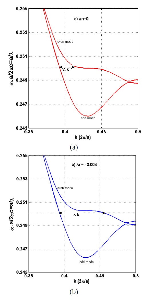
Band diagrams of the proposed switch based on the designed parameters calculated in the previous Section are illustrated in FIG. 3. It shows how the changes in refractive index of polymer in the slot shift the band diagrams of even and odd modes. A small decrease in refractive index causes a large change in even mode’s and a very small change in odd mode’s wavevector at the normalized frequency of
The coupling length
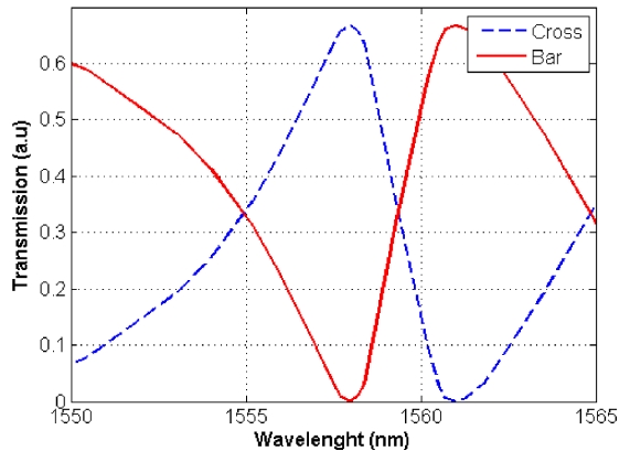
[FIG. 4.] Transmission specrtum of the proposed switch for bar (solid line) and cross (dashed line).

change of the refractive index of the polymer in the slot. The coupling length is almost the same as that of the thermo-optic photonic crystal switch proposed by Krauss
Transmission spectra of the switch are illustrated in FIG. 4 utilizing FDTD method. The power initially transfers through bar ports. A change in refractive index of the structure (which is done by applying voltage to the electrodes), shifts the spectrum, while remaining their shapes [2, 24, 25], causes the structure switches from bar to cross port at the operation wavelength of 1558 nm (corresponding to
Dispersion properties of photonic crystal directional coupler are sensitive to refractive index of the material used in the structure as depicted in FIG. 3. Hence any small change in material refractive index of the photonic crystal directional coupler shifts the dispersion diagram vertically and causes a big change in wavevector of the even mode which causes
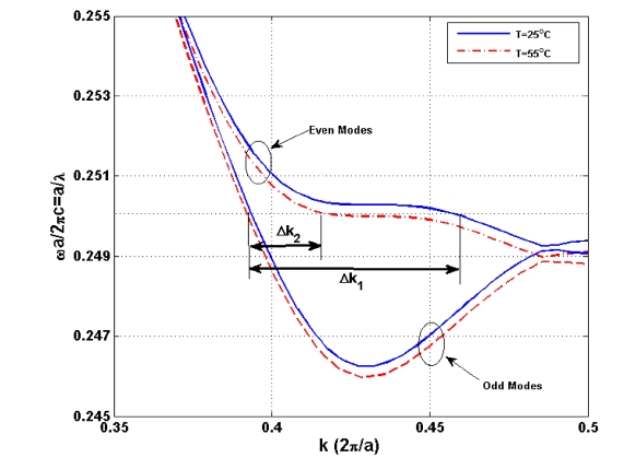
range [1, 30]. The importance of the temperature control in the SPCDC is illustrated in FIG. 5. It shows the changes of the dispersion diagram of the even and odd modes of the proposed structure of FIG. 1 for two different temperatures. The dispersion diagram at room temperature is depicted by a solid line, while the dispersion diagram of the same structure with the same holes and slots filled by polymer, without using negative thermo-optic coefficient of polymer at T = 55℃ is depicted by dashed line. It shows a large decrement of
New compensation method for temperature sensitivity introduced by Chung
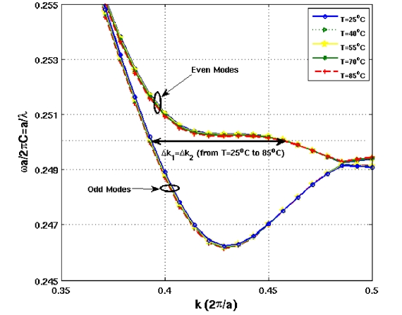
A new design concept of the temperature independent electro-optic switch based on silicon photonic crystal directional coupler (SPCDC) has been introduced. We have maximized the slow light effect in the device by engineering the dispersion properties of the structure to shorten the switching length. Dispersion engineering of the photonic crystal directional coupler has been attained by changing the radii of the innermost rows of the holes in SPCDC and injecting polymer in the slot. Optimum values of the structure parameters have been obtained. Compact length, higher switching speed compared to those of the thermo-optic switches, low activation voltage, easy fabrication and thermal independent switching lengths are the main advantages of the proposed switch. Accurate design and thermal compensation of the polymer makes the performance of the proposed structure stable in the temperature range of 60℃.