While on-chip information processing can efficiently speed up by employing photonic integrated circuits (PICs), there was a significant challenge to realize them by a density comparable to the electronic counterparts due to the presence of the optical diffraction limit. Surface plasmon-based photonics or plasmonics, a recently emerged device technology, can propose a solution to this dilemma, because plasmonics has both the large data carrying capacity of photonics and the miniaturization of electronics [1-3]. Although surface plasmon polaritons (SPPs), surface electromagnetic waves coupled to collective oscillations of free electrons in a metal [4], were first theoretically proposed in 1957 [5], the significant growth and interest in plasmonics is formed since Ebbesen first reported the extraordinary optical transmission through a 2D metallic hole array in 1998 [6]. Nano fabrication techniques, such as electron-beam lithography and focused ion beam milling can be implemented to pattern metallic structures at the nanoscale and make it possible to study the interaction of these nanostructures with light [7, 8].
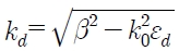
The strong localization of SPPs at the metal-dielectric interfaces has attracted tremendous interests of researchers to SPP-based subwavelength guiding components [9] such as arrayed nanoparticles [10], V-grooves [11], wedges [12], nanowires [13], dielectric-loaded metal films [14] and plasmonic slot waveguides [15]. Among them, Metal-Insulator-Metal (MIM) waveguides are promising in design of a variety of nanoscale plasmonic devices because of possessing high group velocity over a wide frequency range from DC to visible, strong confinement of light waves and also simple fabrication and integration into optical circuits [16, 17]. Although Insulator-Metal-Insulator (IMI) waveguides have the advantage of less loss for the longer propagation distance, but their light confinement capability into subwavelength scales is poor [18]. Numerous functional plasmonic MIM structures like directional couplers [19], filters [20], Y-shaped combiners [21], sensors [22], U-shaped waveguides [23], Bragg reflectors [24], etc, have been numerically and/or experimentally investigated.
Refractive lenses are one of the most ubiquitous optical components with applications ranging from imaging to concentrating light, but their light confinement capability deteriorates as their size approaches the wavelength of light due to the diffraction limit. Surface-plasmon based lenses or plasmonic lenses as an alternative to the ordinary refractive lenses are capable of super focusing beyond the diffraction limit and have great applications in optical data storage, nanofabrication, single molecular biosensing, circular polarizer analyzer and etc [7, 25-27]. Single subwavelength slit surrounded by surface corrugation [28] or by chirped dielectric surface gratings [29], chirped circular slits corrugated on metallic film [30], quasiperiodic array of nanoholes [31] and nanometric cross-shaped aperture arrays [32] in a metal screen are some of the reported design principles to implement the focusing capability of plasmonic lenses. Nanoslits perforated on thin metallic films are recently employed to manipulate the phase front profile [33-35]. The phase shift experienced by light passing through nanoslits is sensitive to its width and depth and also the refractive index of incorporated material. The required phase front profile for focusing action can be achieved by appropriate adjustment of the properties of each slit.
Active control of plasmons which is one of the greatest challenges in recent years is needed to achieve tunable plasmonic devices, besides that, more specifically; the ability to control light with light is required in all-optical signal processing in PICs and optical computing. This can be realized by employing active materials whose properties can be altered by some form of stimulation [3, 36]. Switches and modulators on the basis of the electro-optic effect [37, 38], the magneto-optic effect [39], the thermo-optic effect [40], the plasma dispersion effect [41], the plasmonic excitation of quantum dots [42] and the Kerr nonlinearity [43] are investigated. In the plasmonic lenses formed by nanoslits perforated on thin films, modulating the output beam can be accomplished by incorporating nanoslits with a type of active material like Kerr nonlinear material [44] or anisotropic nematic liquid crystal [45].
In this paper we numerically explore the focusing effect of a plasmonic lens formed by nanoslits perforated on a thin metallic film with slanted cuts on the output surface and incorporated by Kerr nonlinear material. The performance parameters of the proposed lens including focal length (FL), depth of focus (DOF) defined at the half maximum intensity, full-width half-maximum (FWHM) and the efficiency of focusing are investigated. The lens is illuminated by a Gaussian beam and plane wave and the possibility of tuning the focal length by the intensity of incident light and the beam waist of the Gaussian beam is investigated.
This paper is organized as follows; In Section 2 the structure of proposed lens and the analysis method are presented. Section 3 elucidates results of the detailed simulations of the lens and the conclusion will be in Section 4.
II. DEVICE STRUCTURE AND ANALYSIS METHOD
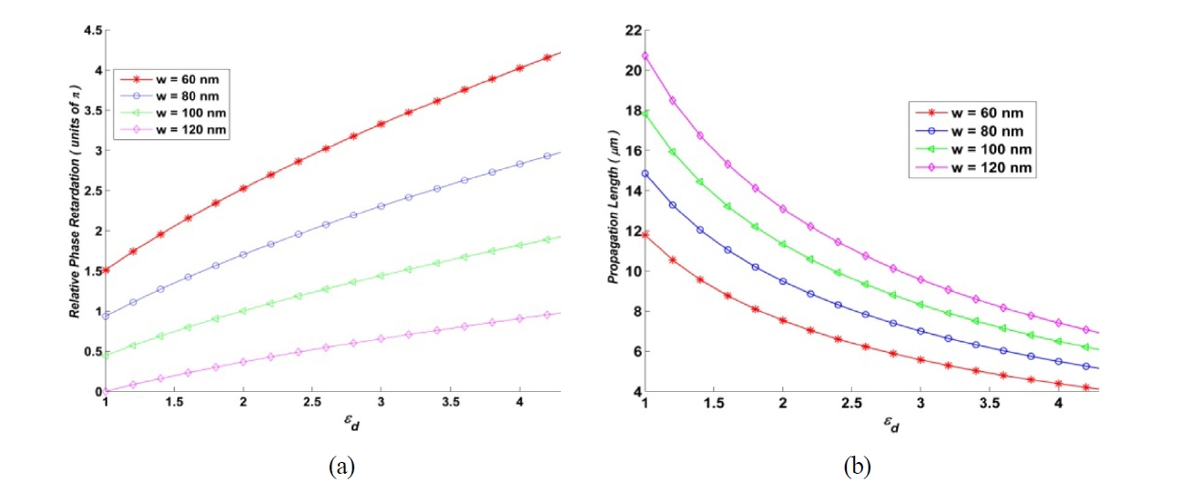
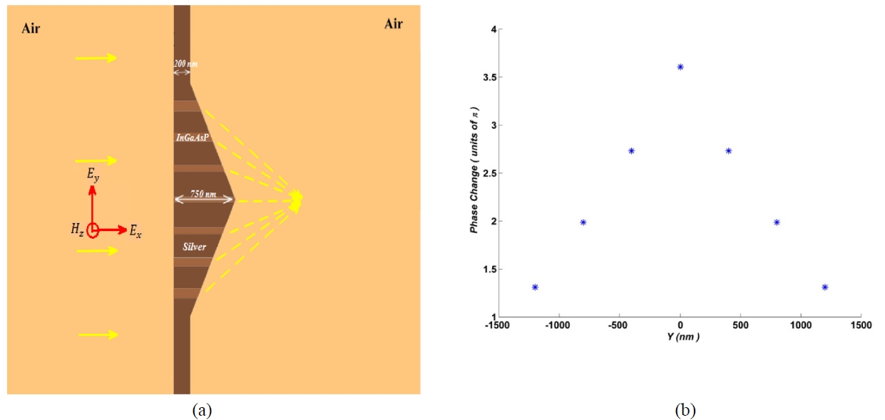
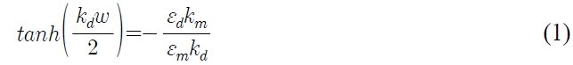
The simulated structure is displayed in Fig. 1(a). The slit widths in consequence from top to bottom are 120, 100, 80, 60, 80, 100 and 120 nm with 400 nm center to center spacing between any two adjacent slits. The underlying physics involved in design of our proposed lens can be discussed as follows. A narrow slit surrounded by metallic walls is the basic building block of the lens. If the space between every two adjacent slits is much more than the metal’s skin depth at operating wavelength, these slits can be assumed as isolated MIMs besides that the slits widths in our structure are much smaller than the operating wavelength, so just the propagation of fundamental SPP mode in MIM waveguide is considered. The complex propagation constant
Where
and
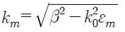
are the propagation constants of the dielectric and metal respectively.

Where
The performance of the proposed lens has been simulated by a two-dimensional nonlinear-dispersive finite-difference time-domain (2D N-D-FDTD) numerical method, assuming the slit lengths (in z direction) to be infinite. This assumption is acceptable for slit lengths larger than 15 μm [46] and by using the fact that the error in 2D simulations in comparison with 3D simulations will be negligible (Less than 10 percent). Obviously more accurate results by investigating the effect of finite slit length can be obtained by 3D N-D-FDTD but at a cost of large amounts of computer memory and increased computing time. The outer boundary of the computation lattice is terminated to the convolutional perfectly matched layer (CPML) to dissipate outgoing waves [47]. The second-order Lorentz dispersion model is employed to characterize the frequency-dependent relative permittivity of silver, when time dependency is taken
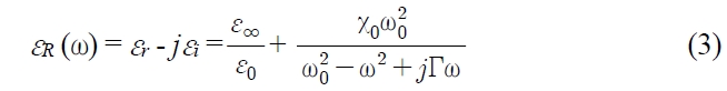
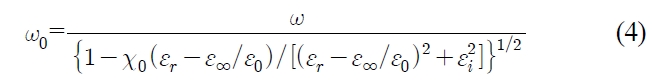
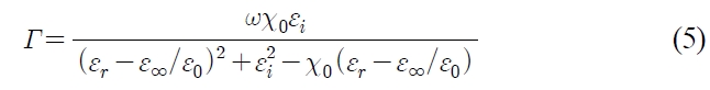
Where ω0 and Γ are resonant frequency and damping coefficient.
A TM-polarized plane wave of 850 nm wavelength consisting of

achieved by Courant stability condition, where
The nanoslits are filled with Kerr nonlinear material. For a Kerr nonlinear medium the dielectric constant

The linear dielectric constant
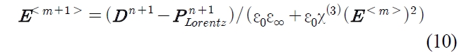
To simulate the performance of proposed lens, at first step, The electric flux density D is obtained by solution to Maxwell’s equations; ∇×

Where ε0 is the free space permittivity,


Where
Where

Where
that has a solution for
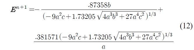
This result is used in following simulations and provides more accuracy than the first method for few iterations.
III. SIMULATION RESULTS AND DISCUSSION
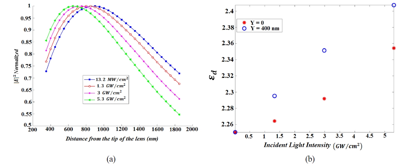
As mentioned previously, change in the dielectric constant of incorporated material in nanoslits can be implemented to modulate the output beam. For different values of
The nanoslits in our structure are filled with Kerr nonlinear material. By increasing the intensity of incident light, in the situation that Fabry-Perot (F-P) resonances
occur in the slits in the result of impedance mismatch at the entrance and exit surfaces of each slit, the dielectric constant of incorporated nonlinear material increase. By increasing
The results depicted in Fig. 4(a) illustrate the movement of focal point toward lens by increasing the intensity of incident light, which is in the result of formation F-P resonances in three central slits, while the outer slits remain out of F-P resonances. Figure 4(b) represents the dependence of the dielectric constant of incorporated Kerr nonlinear material in nanoslits located at y=0 and 400 nm to the incident light intensity.
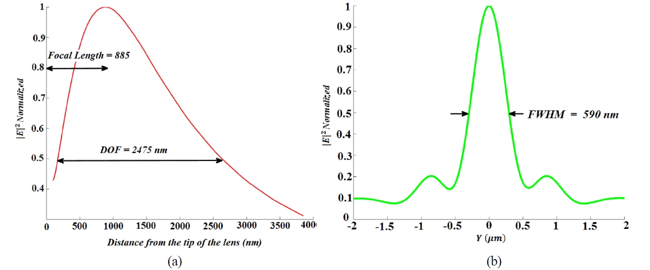
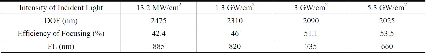
Table 1 lists the focusing properties of the lens for different values of incident light intensity. FWHM is approximately unchanged and remains equal to 590 nm for all four cases but the DOF parameter which determines the working distance for beaming application, decreases.
Certainly, rather than the absorption of a portion of light in the structure, there is reflection of light from the surface of the lens in the illuminated side, so the proposed lens cannot transmit 100% of the incident light. Also, it should be pointed out that in these kinds of lenses which are formed on the basis of nanoslits perforated on thin metallic films, because of the low decoupling rate of surface plasmon modes to propagating electromagnetic wave modes, most of the energy remains at the output surface of the lens and hence the efficiency of energy passing through the lens will be much more than the efficiency of focusing [25]. The efficiency of focusing which is obtained by dividing
Performance parameters of the proposed lens for different values of incident plane wave intensity
the intensity of focal point to the incident intensity increases by increasing the incident light intensity; attributed to the formation of F-P resonances in central slits and the results are also presented in Table 1.
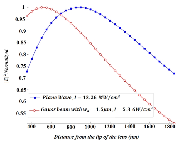
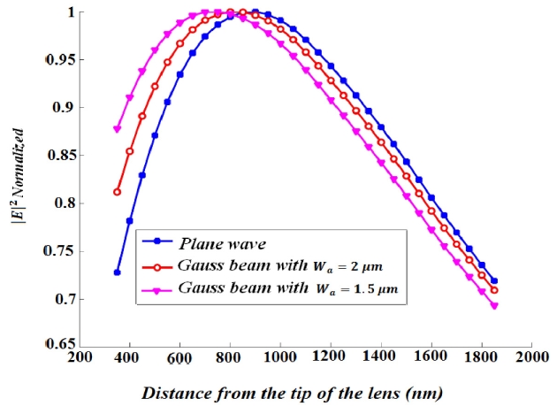
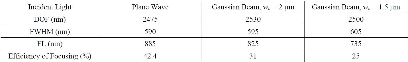
In comparison with the situation of illuminating the lens by a plane wave, when the lens is illuminated by a Gaussian beam, the central slits provide more phase retardation and hence the focal length decreases. Also the amount of decrease in focal length depends on the beam waist of the Gaussian beam which is shown in Fig. 5.
The performance parameters of the lens for the cases of illuminating the structure by plane wave, Gaussian beam with beam waist of 2 μm and 1.5 μm are listed in Table 2.
We are limited in how much we can increase the incident
Performance parameters of the proposed lens for the cases of illuminating the lens with plane wave, Gaussian beam with wa = 2 μm and wa = 1.5 μm
light intensity to reduce the focal length, but we can increase the maximum change in focal length by employing a Gaussian beam. Our simulations reveal that when the structure is illuminated by 5.3 GW/cm2 Gaussian beam with 1.5 μm beam waist and plane wave the focal length will be 515 and 660 nm respectively, so if illuminating the structure by 13.2
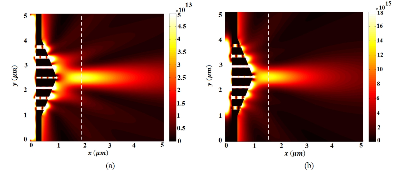
MW/cm2 plane wave be considered as the initial situation, the maximum change in focal length increases 64% in the case of employing a Gaussian beam instead of a plane wave as is shown in Fig. 6.
Time?average electric field intensity distribution |E|2 for two cases depicted in Fig. 6, are presented in Fig. 7.
The maximum intensity of incident light in our simulations is 5.3 GW/cm2 which is below the threshold that can result in material damage, but temperature increase as the result of optical absorption, should be considered. Electron thermal dynamics induced by the interaction of a high intensity light with a metal can be precisely described using the Two-Temperature Model. Two temperatures refer to that of the electrons (
In conclusion, the performance of a plasmonic lens composed of an array of nanoslits introduced in thin metallic film with slanted cuts on the output surface and filled with Kerr nonlinear material has been explored. The performance parameters of the lens for the cases of illuminating by plane wave and Gaussian beam with different intensity and beam waist have been investigated. An exact formula for obtaining electric field