Recently long-wavelength vertical cavity surface emitting lasers (LW VCSELs) operating at 1.3 μm and 1.55 μm wavelengths have made significant progress for potential applications for optical transmitter sources in local and access networks and in optical interconnects [1-10]. The importance of the VCSEL devices is better recognized these days as low power consuming optical signal sources in information technology (IT) systems. Beside the low power consumption property the VCSELs have many other advantageous characteristics, such as pure single-mode lasing, easy coupling to optical fibers, low manufacturing cost and wafer-level testing, compared to the existing edge-emitting laser diodes. Technologies on the LW VCSELs based on InAlGaAs/InP expitaxial wafers have been developed significantly during the last several years. High-speed modulation and fiber transmission of the devices over long distances up to 100 km have been reported in the literature [11,12]. A vertical stack of appropriately distributed Bragg reflectors (DBRs) made of GaAlAs-InAlAs or InP/Air layers was used for the InAlGaAs/InP LW VCSEL cavities of high temperature characteristics and efficient current confinement schemes with a suitable tunnel junction aperture [13,14]. However, there have been few commercial products available for high-speed (equal to or above 10 Gb/s) InAlGaAs/InP based LW VCSELs. The previously reported results on high-speed LW VCSELs are mostly related to the VCSELs fabricated either by molecular-beam epitaxy (MBE) grown epitaxial technologies [13-15] or by wafer bonding methods [17,18]. The MBE method is known to be not as good as the metal-organic chemical vapor deposition (MOCVD) method for mass production of the VCSELs, and the wafer bonding technology is also not as easy as the epitaxial growth technology for the VCSEL fabrication. This may be one of the major reasons that the reported high-speed LW VCSELs are not readily available in commercial markets.
In this experimental study, we evaluate 10 Gb/s data transmission performance of 1.3 μm wavelength VCSELs whose bottom and active layers were grown by an MOCVD method in a one-step epitaxial growth process and whose top reflecting layer was formed with a dielectric mirror. The MOCVD technology is proven to be useful for massproduction and for reliable epitaxial materials [5-10]. Results obtained for error-free data transmission over 10-km singlemode fiber (SMF) in various temperature conditions by using the direct modulated VCSELs at a bit rate of 10 Gb/s with a pseudorandom binary sequence (PRBS) of 231-1 bit length are described in the following sections.
II. CHARCTERISTICS OF THE VCSELS
We used a pigtailed 1.3-μm VCSEL, which was designed, manufactured and packaged by RayCan Co. Ltd., in Korea, as a light source for 10 Gb/s data transmission over a 10-km long SMF. The VCSEL was an InAlGaAs/InP-type with a tunnel junction and an air-gap aperture. The MOCVD technology was used to grow the whole epitaxial layer structure with a 0.5-
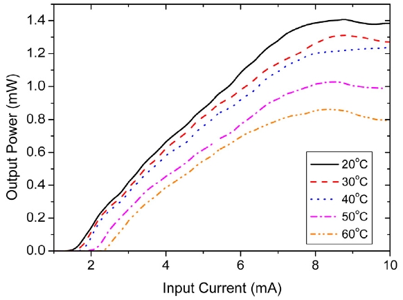
Figure 2 shows the continuous wave (CW) lasing characteristics of the single-mode fiber pigtailed InAlGaAs VCSEL emitting 1.3 μm wavelength light as a function of the bias current at various temperatures. The single-mode output power at each temperature continued to increase up to the bias current of 8 mA, and then saturated above that. The output power at a temperature of 20℃ was 1.38 mW when a current of 8 mA was applied. As the temperature
increased from 20℃ to 60℃, the output power at the current of 8 mA decreased from 1.38 mW to 0.85 mW, whereas the threshold current increased from 1.5 mA to 2.3 mA. The high slope efficiencies of 0.24, 0.22, 0.20, 0.17 and 0.15 W/A at an input current range of 5 mA, which was above the thresholds, were achieved at temperatures of 20, 30, 40, 50 and 60℃, respectively. Variation of the VCSEL’s bias voltage and series resistance with temperature change was around 5% and 10%, respectively. The series resistance of the VCSEL at the operation current of 7 mA was around 70 Ohm.
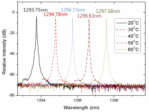
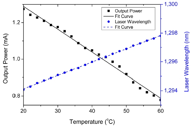
The optical spectra of the VCSEL output taken at the driving current of 7 mA for various temperatures are shown in Fig. 3. The resolution of the spectrum measurement was 0.07 nm. The measured results show that the CW lasing wavelength is shifted by approximately 3.8 nm for 40℃ temperature change. The temperature coefficient of the lasing wavelength is about 0.096 nm/℃. The black trace represents the peak lasing wavelength of 1293.75 nm at 20℃, while the following dotted and dashed traces represent the peak lasing wavelengths of 1294.78 nm, 1295.73 nm, 1296.63 nm, and 1297.58 nm at 30, 40, 50 and 60℃, respectively. Figure 4 describes plots of the measured VCSEL output power and peak laser wavelength
at a fixed driving current of 7 mA as functions of temperature.
III. OPTICAL FIBER TRANSMISSION EXPERIMENTS
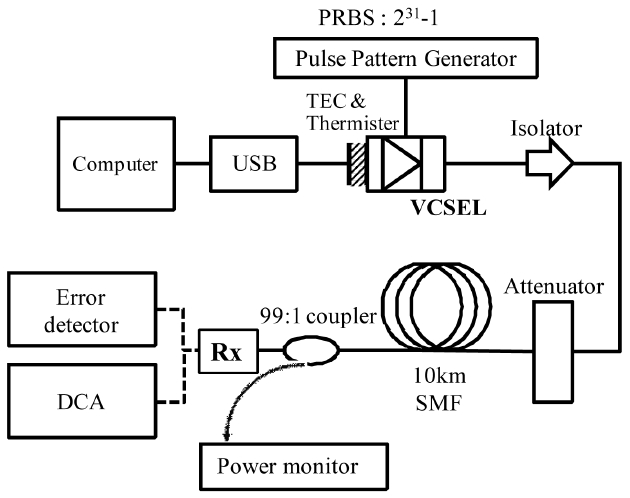
The schematic diagram of an experimental setup used for the measurement of the VCSEL’s optical transmission characteristics is shown in Fig. 5. We used an integrated board (custom designed by BiOptics Co., Ltd.) for the control of the direct current (DC) bias with an integrated bias tee having a modulation signal input port and for the control of the operating temperature of the VCSEL with a pair of internally packaged TEC and thermister in the TO-CAN. The board was interfaced with a computer with a USB cable and was controlled with a computer program. It provided an optimized DC bias and modulation current
input as well as an improved high-frequency modulation signal transfer capability. The VCSEL was driven by a pulse pattern generator (PPG, Anritsu MP1763C) with a Non-Return-To-Zero (NRZ) modulation data signal having a 231-1 PRBS pattern. For 10-km long SMF transmission experiments, a DC bias current of 7 mA and a modulated current of 6 mA were applied to the VCSEL at temperatures of 20, 40, and 60℃. An optical isolator of 0.25 dB insertion loss was used right after the VCSEL to prevent back-scattered optical beams from feeding back into the VCSEL and deteriorating the VCSEL performance. A 99:1 splitter was placed after the 10-km long SMF to tap out the transmitted VCSEL optical signal through its 1% output port for measurement of bit-error-rate (BER) of the transmitted signals as a function of the received signal power. The received eye diagrams and BER were recorded using a digital communications analyzer (DCA, HP 83480A) and a bit error detector (Anritsu MP1764C), respectively. We compared the eye diagrams and BER data for the back-to-back (BTB) transmission condition with those after 10-km long SMF transmission which had an optical attenuation of 0.326 dB/km at the 1310 nm wavelength. For the BER measurement a receiver board with a PIN photodiode (fabricated by Lightron Optoelectronics Co., Ltd.) optimized for detection of 10 Gb/s data streams was used.
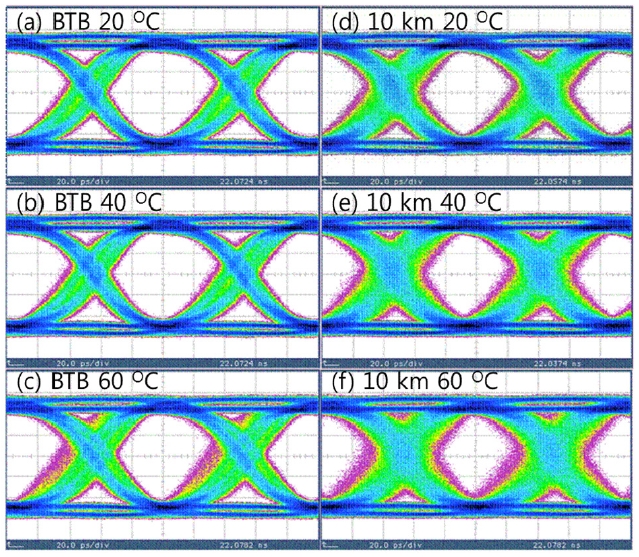
The measured eye diagrams using a 10 Gb/s receiver board with a PIN photodetector are shown in Figs. 6(a) through (f). The receiver board was used to convert the transmitted VCSEL’s light beam signal into electric signals.
The VCSEL used in this experiment was directly modulated at a bit rate of 10.3125 Gb/s. We measured eye diagrams of the VCSEL output with the receiver board directly connected to the VCSEL for the BTB transmission test and those after transmission over a 10-km long SMF at various temperatures. Figs. 6(a)~(c) indicate the BTB eye diagrams at 25, 40, and 60℃, respectively, whereas Figs. 6(d)~(f) correspond to the eye diagrams after the 10-km long SMF transmission at the three temperatures. Clear open eyes were observed for both cases of the BTB and of 10-km long SMF transmission for the three temperatures. The measured diagrams show that smaller eyes due to larger timing jitter and amplitude fluctuation are observed for the SMF transmission than those for the BTB case. The timing jitter and amplitude fluctuation are affected more significantly by the fiber transmission than by the temperature increase.
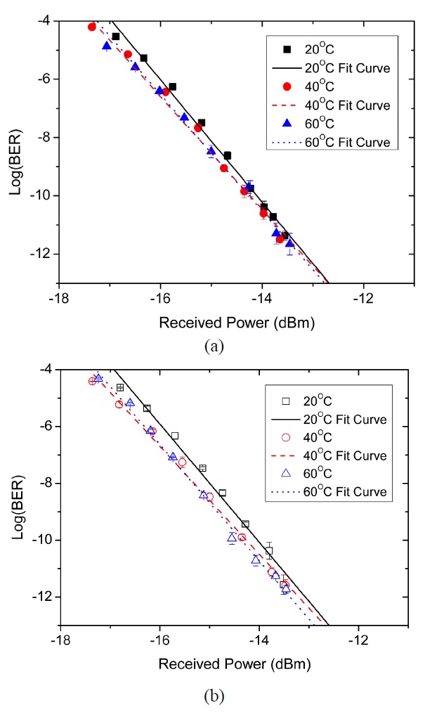
The BER measurement was conducted four times for each of the BTB and 10-km long SMF transmission at each temperature condition. The average values with error bars corresponding to the standard deviation of four measured data were plotted in Figs. 7(a) and (b). Successful error-free transmissions were possible up to BER of 10-12 with the 1.3-μm wavelength single-mode VCSEL under all conditions, even at the operating temperature of 60℃, for input data stream of PRBS of 231-1 bit length. Filled symbols in Fig. 7(a) indicate the measured BER data for the BTB cases, and open symbols in Fig. 7(b) indicate those for the 10-km-long SMF transmission cases. Each of the three different shape symbols corresponds to data taken at each of the three different operating temperatures, and three different-type lines are used for curve fitting to each set of
the data points. For the uncompensated transmission over the 10-km-long SMF, the error-free condition was achieved at the received power level of approximately -13.4 dBm for an error rate of 10-12. The measured results indicate that there is no significant difference between the BER curves for the operating temperatures up to 60℃ and no notable power penalty is observed even after the 10-km long SMF transmission compared to the BTB cases. The error bar of the BER data, which corresponds to the standard deviation for the run-to-run measurements at each operating condition, is shown to be relatively very small or comparable to the symbol size except for a few cases as plotted in Figs. 7(a) and (b).
We have evaluated 10 Gb/s data transmission characteristics of a directly modulated single-mode InAlGaAs/InP VCSEL of 1.3 μm wavelength for a 10-km long SMF without any kind of optical or electrical dispersion compensation. The VCSEL’s bottom DBR and central active epitaxial layers was grown monotonically with MOCVD method, and the top DBR mirror was formed with a dielectric coating process. Error-free transmission of the directly modulated VCSEL’s output over the 10-km long SMF was achieved at optical received power of around -13.4 dBm up to the BER of 10-12 within a temperature range of 20~60℃ only with a DC bias current of 7 mA and modulation current of 6 mA. The experimental results indicate that the InAlGaAs-InP VCSEL grown by the MOCVD could be a low cost, reliable and low power consuming optical signal source for optical fiber communications at the wavelength of 1.3 μm. It can also be concluded that the VCSEL is a potentially good optical transmitter source for 10 GBASELR and -LW Ethernet applications under controlled environments.