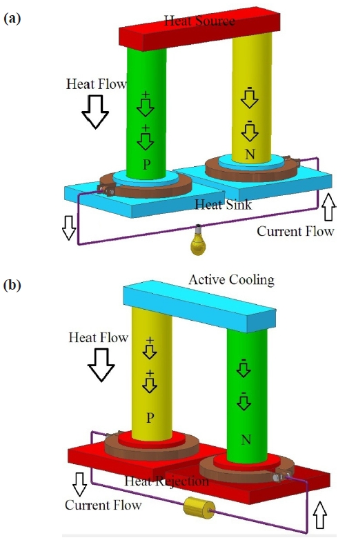
The dependence on fossil fuels for most of our energy needs has become a serious issue due to the adverse effect on global economy brought by the increasing costs and the volatility of the fuel market. The negative impact on global warming is a long term issue pushing attention to alternative, cleaner, and cheaper energy sources. In this regard, harvesting solar and wind energy sources is a major focus throughout the world, and to a lesser extent, recapturing waste heat as power offers a solution to many our energy problems. In many scenarios in daily life, heat is just dissipated without deriving any benefit, for example, the heat produced by the car engine. Thermoelectric materials have made it possible to convert that thermal energy into electrical energy [1-5]. The reversible process of refrigeration is also possible by supplying an electrical current to produce a thermal gradient (Fig. 1 ). Thermoelectric devices do not have moving parts, create pollution, or make noise, thus offering an attractive source of en-ergy.
A thermoelectric device is a combination of p-n junctions which are connected electrically and thermally in series and parallel respectively. Many such p-n junctions are needed to generate the desirable output voltage since each p-n junction in a system only generates a small voltage difference. Bulk ther-moelectric materials do not have high efficiency, limiting wide applications at present. The figure of merit for a thermoelectric material, ZT, is given as:

where S is the Seebeck coefficient, σ is the electrical conduc-tivity, T is the temperature and κ is the thermal conductivity. The product S2σ is also known as power factor. There has been a tremendous amount of research in the last decade to improve the ZT beyond that of bulk materials. Nanomaterials appear to provide an avenue to achieve this goal, for example, making nanocomposites, adding nanoparticles to a bulk material, or em-ploying one-dimensional nanostructures. Significant amount of research has been reported [6-11] on nano/micro-grained com-posites and adding nanopaticles to a bulk thermoelectric mat-erial.However, this review does not cover these developments but focuses only on the use of nanowires in thermoelectric power generation. A background on the physics of thermoelectricity is given first, followed by conventional devices. The rationale for using nanowires in this endeavor and the current status are discussed next and finally, a summary of challenges and future
outlook is presented.
2. BACKGROUND ON THERMOELECTRICITY
In 1821, Thomas Johann Seebeck discovered the thermo-electric effect while doing a simple experiment using a circuit made from two different metals, with the junctions maintained at different temperatures. He noticed that this would deflect a compass magnet and later realized that a "thermoelectric force" induced an electrical current, which according to Am-pere's law deflects the magnet. Thermoelectricity is attributed to the thermal diffusion of charge carriers in a material. Hot charge carriers in a thermoelectric material diffuse to the cold end of the material much more than the cold charge carri-ers diffusing to the hot end, and this proceeds until a state of dynamic equilibrium is reached. This phenomenon is known as the Seebeck effect. The voltage is proportional to the tem-perature difference between the two junctions. This relation between the temperature difference and the output voltage de-fines an important parameter called the “Seebeck coefficient”, or thermopower. Themoelectric power (TEP), S (units: μV/K) is one of the basic characteristics of a material; similar to other properties of a material such as electrical conductivity, it can be measured and classified for a material. The thermoelectric voltage can be either negative or positive depending on if the holes or electrons are charge carriers. The Seebeck coefficient is given by:

Several years after Seebeck’s experiments, a French physicist in 1834 discovered that a current passing through a junction of two dissimilar metals produced heating or cooling. It was pos-sible to freeze water into ice or melt a cube of ice, depending on the direction of the current. The heat created (or absorbed), q, is proportional to the current, I and the coefficient relating the two is called the Peltier coefficient.

The Seebeck coefficient and electrical conductivity depend only on the electronic properties of the material whereas the thermal conductivity depends on contributions from both the electronic component and lattice vibrations. Achieving high ef-ficiency requires a high S to realize a large voltage for a small temperature difference, a high σ to minimize Joule heating losses, and a small κ to maintain a high temperature difference.In reality, it has been very challenging to reach a high ZT (for ex-ample ZT >1) since the parameters mentioned above are not in-dependent of each other, and any attempt to improve one might adversely affect the other. For example, an increase in electrical conductivity invariably accompanies an increase in thermal conductivity. A thermoelectric device with a ZT higher than 3 is necessary to be competitive with conventional refrigeration or power generation.
Semiconductor materials exhibit high Seebeck coefficients which makes them attractive as efficient heat pumps. While the best metal has a Seebeck coefficient of ~ 30 μV/K, some semicon-ductors have Seebeck coefficients in the range of 100 - 200 μV/K. In metals, only a small fraction of electrons at high energies are capable of changing energy states and exchanging energy with the surrounding environment according to the Pauli Exclusion Principle. This fraction can be predicted using Fermi-Dirac sta-tistics:
where ζ0 is the Fermi energy [2]. For semiconductors, because of the energy gap, Maxwell-Boltzmann statistics can be used to approximate the number of elec-trons contributing to an electronic specific heat.
where U is the excitation energy per electron [2]. The second term in the above equation implies that the number of charge carriers in the conduction band will go up when the temperature increases. The electrons in the relatively empty conduction band in semiconductors are more capable of changing energy states than in the case of metals which causes an increase in the elec-tronic specific heat.
SiGe, PbTe and Bi2Te3 alloys are some of the popular semicon-ductor materials considered for ther-moelectric applications. In principle, there is no theoretical limit for the efficiency of a thermoelectric device, however, practical considerations such as the limitation in the ratio of σ/ κe (where κe is the electronic contribu-tion to the thermal conductivity according to the Weidmann-Franz law) make it hard to improve the efficiency. Consequently, the larg-est ZT value realized to date in applications is around 1 for Bi2Te3.
A bulk semiconductor with a high atomic weight and a rea-sonable S and σ is expected to have a low thermal conductivity, resulting in a large ZT. This expectation is due to the reduced speed of sound in such a material, but this has not been realized yet [12]. New bulk materials with higher ZT have been under in-vestigation in recent years. Rhyee et al. [13] reported a ZT of ~ 1.5 at 705 K in a binary crystalline bulk n-type In4S3-δ attributing the high value to the high Seebeck coefficient and the low thermal conductivity in the plane of the charge density wave.
The efficiency of a thermoelectric element is related to ZT as follows [14]:
where

is the Carnot efficiency, which places a fundamental limit on the efficiency of all heat engines. The efficiency of a thermoelectric device would reach the Carnot limit only with an infinite ZT according to this relation.
4. CURRENT THERMOELECTRIC APPLICATIONS
Currently, a variety of thermocouples, Petlier coolers and even automobile seat warming/cooling systems made of thermoelec-tric materials are available in the market. Thermoelectric genera-tors have been used in satellites and space probes. For example, in a “radioisotope thermoelectric generator” (RTG), radioactive decay releases heat and an array of thermocouples convert this heat into electricity through the Seebeck effect. Plutonium-238 as oxide Pu02 is used in this system which emits alpha particles during the isotopic decay process and the emitted particles col-lide with the walls of the containers, creating the heat for the thermoelectric converter [15]. Such devices have been developed and implemented by NASA in various space missions including Apollo, Pioneer, Viking, Voyager, Galileo, and Cassini.
For the automotive sector, Amerigon Inc. designed and fabri-cated a climate control seat system used in the front seat on two models of the Jaguar XF mid-size luxury sports sedans, as well as the Nissan Maxima. This system allows the driver to warm or cool the seats as needed seasonally [16]. Other commercialized devices include water coolers, cool/heat sleep pads, and per-sonal mini coolers [17]. A Japanese company recently developed [18] a device for charging cell phones, lap tops, etc., with the pur-pose to help people who have lost their homes due to the 2011 tsunami in Japan. A pan in this device contains a thermoelectric material at the bottom with one end in direct contact with the fire while the other end has an interface with the boiling water in the pan. The average temperature of the fire is ~ 600℃ and with water boiling at 100℃, the difference in temperature can be used to produce electricity.
5. NANOMATERIALS FOR THERMOELECTRIC APPLICATIONS
Nanomaterials have renewed the interest in thermoelectricity by allowing to tailor the interdependent parameters, thus pro-viding new avenues to increase the efficiency of thermoelectric devices [19,20]. Low thermal conductivity and a wide range of density of states and phonon electron scattering in nanomaterials make them ideal for thermoelectric applications [21,22]. When the dimensions of a material are about the mean free path of electrons, the density of states increases due to quantum confinement [23], which causes an increase in the Seebeck coef-ficient [24]. Moreover, the thermal conductivity of the material decreases due to the surface scattering mechanism, since the dimensions are less than the mean free path of phonons.
Alloying used to be the main approach to achieve increased ef-ficiency. Since the 1990s, two different alternatives have become popular: the first one involving new materials with complex crystalline structures and the second by reducing the size of the candidate material [25]. Simple alloying was replaced by nano inclusions when the field of nanotechnology started to receive attention, following theoretical predictions that nano-inclusion reduces the thermal conductivity more than alloying [26]. Tuning of the transport parameters has been shown to be possible in the case of microstructural modifications in nano/micro compos-ites. When the grain size increases, the carrier mobility increases resulting in an increase in electrical conductivity. It is also practi-cal to reduce the thermal conductivity by increasing the grain boundary scattering [25].
Dresselhaus et al. [23] first reported the possibility of increasing the power factor by taking advantage of quantum confine-ment effects. Since then, research on different low-dimensional systems including superlattices, nanowires, and quantum dots has intensified. Venkatasubramanian et al. reported a ZT of 2.4 for Bi2Te3/Sb2Te3 [27] by controlling the transport of phonons and electrons in the superlattices; a temperature drop of 32 K was shown possible at room temperature in a device using this material. Harman et al. obtained a ZT larger than 3.0 at 600 K for PbTe/PbTeSe quantum dot superlattices [28].
6. NANOWIRE-BASED DEVELOPMENTS
The single crystalline nature of nanowires is more advanta-geous than superlattice films since the electrical conductivity in nanowires is not limited by charge scattering, tunneling, and hopping [29]. In addition, electrical conductivity can be opti-mized by doping as well. Surface scattering in nanowires [30] changes the lattice component of thermal conductivity (
While size reduction in nanowires confines the movement of the electrons to one direction, it does not restrict the motion of phonons. The motion restriction of electrons improves the electrical conductivity and thus, modifies Seebeck coefficient as desired [30,31]. However, the electronic component of thermal conductivity also increases too, which is undesirable. The lattice component of thermal conductivity can be estimated from:
where νS is the speed of sound in the material and
diameter of the nanowire; then, the thermal conductivity will re-duce with the size of the nanowire.
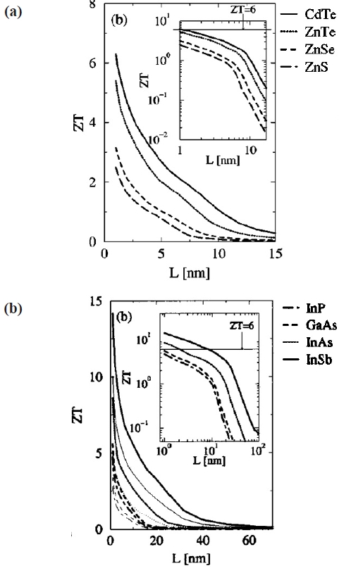
Nanowires have been predicted to show interesting proper-ties for diameters less than 100 nm [32]. Mingo calculated the ZT for various II-VI and III-V semiconductors in bulk and nanowire formss [33,34] using an iterative solution for the Boltzmann transport to model the electronic transport and a full transmis-sion function approach for the prediction of the lattice thermal conductivity. His results showed that (i) ZT increases with a de-crease in nanowire diameter, (ii) CdTe in II-VI semiconductors and InSb in III-V semiconductors are the best choices for ther-moelectric applications, and (iii) II-VI nanowires have smaller ZTs compared to III-V materials for a given nanowire diameter. Based on his predictions reproduced in Figure 2, nanowires with diameters smaller than ~5 nm are needed in order to obtain ZT greater than 3.
Size effects on thermal conductivity and ZT of nanowires have been investigated extensively. A theoretical study [35] based on the Boltzmann transport equation and
tivity of PbSe nanowires was found to be lower than bulk PbSe by a factor of 10-1000 at various temperatures [38].
The potential for obtaining high ZT using heterostructures and hollow nanostructures has been explored by many groups [39,40]. Nano-heterostructures may exhibit a low thermal conductivity due to interface phonon scattering [41]. A core-shell structure is another effective method for reducing the thermal conductivity where the rough interface acts as a secondary scattering phase. Kang et al. [41] reported the possibility to reduce the thermal conductivity of Bi/Te core-shell nanowires to an amount close to the amorphous limit. While the electrical conductivity of the core/shell nanowires does not change appreciably, their ther-mal conductivity can be five times lower than the conventional nanowire of the same size. These findings have also been vali-dated by molecular dynamic simulations [42]. The degradation of thermal conductivity of Si/Ge core/shell nanowires is at-tributed to the depression and localization of long-wavelength phonon modes at the interface of Si/Ge as well as high frequency non-propagating diffusive modes.
Hochbaum et al. [43] reported that rough Si nanowires have a low thermal conductivity around 1.6 Wm-1K-1, attributing it to the higher rates of diffuse reflection or backscattering of phonons at the interfaces. They also showed that Si nanowires smaller than 50 nm in diameter exhibit two orders of magnitude reduction in thermal conductivity. Several experimental and theoretical studies have focused on the effects of growth direction of the nanowires on thermoelectric properties [35,44]. The growth direction affects the charge and energy transport in nanowires. For example, anisotropy in thermal conductivity of single-crystal Bi nanowires has been reported [44], with [110] nanowires showing a thermal conductivity about a quarter of that of

nanowires. Computational studies [35] confirm that electrical conductivity, Seebeck coefficient, and electron thermal conductivity of silicon nanowires are strongly dependent on the growth direction
of the nanowire. Si nanowires with a 1 nm diameter grown in [011] have the highest values of σ and κe for a given carrier concentra-tion.For nanowires with a diameter of 3 nm, wires with a growth direction of [011] show the highest electrical conductivity. These studies indicate the need to consider growth direction in the de-sign of future devices since it can affect the efficiency consider-ably.
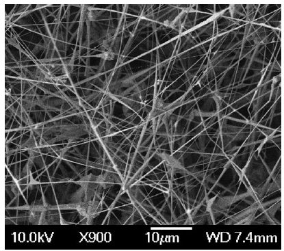
Various methods have been used for the growth of thermo-electric nanowires including sol-gel techniques, template syn-thesis and vapor-liquid-solid (VLS) approach using catalysts [46]. Typically, chemical synthesis techniques performed at low temperatures do not yield high quality nanowires suitable for electronics applications as these structures tend to have many defects. Template-based techniques, while allowing to grow ver-tical nanowires confined into the pores, template removal and possible resultant damages pose an issue in device fabrication. Compared to these two techniques, the VLS approach is more popular since it is similar to chemical vapor deposition except for the use of a catalyst to facilitate nanowire formation [46-48]. Figure 4 shows a mat of ZnTe nanowires grown using VLS method. Regardless of the approach, precise diameter control of the nanowires is currently elusive. Precise positioning of the nanowires with controlled diameters has been attempted using nanoporous templates [49], scanning probe lithography [50], AFM resist scratching and liftoff [51], and nano polymer wires or tubes as templates [52]. Zhou et al. [53] reported that the growth pressure affects the thermoelectric properties of InSb nanow-ires synthesized by the VLS method. The Seebeck coefficient of InSb nanowires is found to be smaller than bulk InSb and nanowires grown at lower pressure have a higher Seebeck coefficient. This observation was attributed to the formation of Sb-doped InSb NWs due to the loss of In, since In is easily oxidized by the remaining oxygen in the growth tube. Their samples also had a thin layer of indium oxide and its effect on the observations made is not clear.
The measured ZT values of nanowires in many cases appear to be lower than theoretical predictions and the main reason may be due to the low measured electrical conductivity of the nanow-ires. The charge carrier mobility of the nanowires is very low due to the surface trap states and point defects. Annealing can possi-bly reduce the defect density [54] and subsequently increase the electrical conductivity. Annealing of p-type PbSe [29] was shown to decrease the resistivity of the nanowires significantly, with the power factor value of ZT reaching 0.04 ohm.cm. The approaches commonly used for making these measurements is discussed next.
Most experimental studies focused on a mat of nanowires for measurement of thermoelectric properties due to the difficulties associated with isolating and positioning a single nanowire [55].
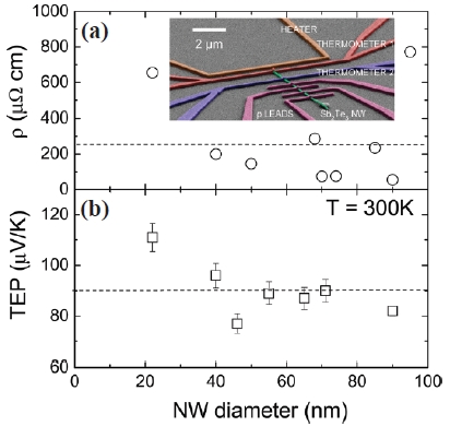
It is not possible then to evaluate the properties as a function of size, impurities, etc. In order to measure the thermoelectric properties of a single nanowire, a test device small enough to make the measurement is needed and two methods have been commonly used in the literature. In the first method, a thick layer of silicon dioxide is formed on the silicon substrate. The low thermal conductivity of SiO2 helps to obtain the required temperature difference between the two ends of the nanowire. Then, several drops of the nanowire dispersion are placed on the substrate and after the solvent evaporates in a few minutes,the nanowires remain on the substrate. Subsequently, gold (or Pt) electrical contacts are fabricated using photolithography and electron beam evaporation. One of the electrodes acts as a heater, and Joule heating through a heater line is used to estab-lish a temperature difference which generates a thermoelectric voltage in the nanowire [56-58]. The Seebeck coefficient of the nanowire is calculated using ΔT and measuring the Seebeck volt-age. Though this approach is simple and provides good electrical contacts, it is difficult to establish a large temperature difference between the two ends of the nanowire since the nanowire is on a huge thermal mass of silicon oxide (Fig.5 ). Thermoelectric prop-erties of individual single crystal antimony telluride nanowires of varying diameters were measured using such a device [59] which showed that the resistivity of the nanowires is close to the bulk value. An increase of 30% for thermopower was seen for thin nanowire due to hole-dominant diffusive thermoelectric genera-tion.
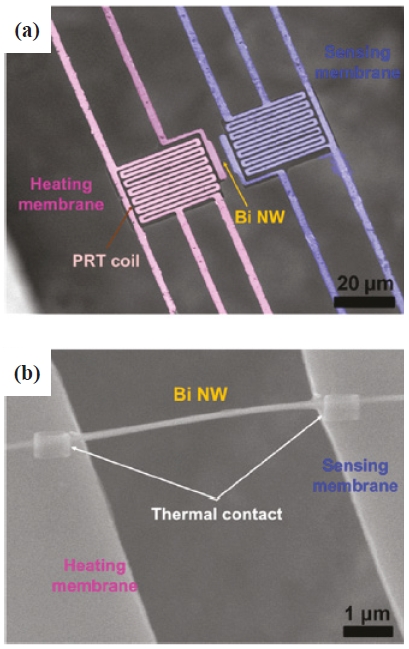
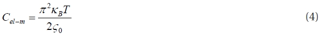
The second method has addressed the shortcomings of the method mentioned above by suspending the nanowire [60,61] as seen in Fig. 6 A higher temperature gradient can be maintained since the sensing points are suspended. Thermal conductivity is calculated by considering the diameter and the conduction length of the nanowire between two suspended structures, and the difference in temperature between the two ends [38]. Be-cause of the complexity of the measurement device and sequen-tial fabrication steps, a nanowire is picked from the bulk sample and placed on the fabricated device. A few additional steps are required after placing the nanowire, such as focused ion beam deposition of platinum to make the electrical contacts [60,61] and fixing the nanowire in its place (Fig.6 (b)). This approach provides good electrical contacts [62] which is critical to make re-liable measurements. The accurate positioning of the nanowires on the suspended devices is a major challenge. One can choose a large enough nanowire visible under a microscope [60] or use a drop or two of a very dilute nanowire dispersion hoping to get by
chance a single nanowire [63-65]. Direct growth of the nanowire on the device has also been suggested but usually ruled out due to the high temperatures involved in the growth process [61].
The potential of nanowires to construct thermoelectric de-vices with higher efficiency compared to bulk materials and thin films is well recognized at present. The literature on theoretical studies and experimental attempts to make measurements has been extensive as reviewed here. But a glance at this literature and comparing different reports on the same material reveals significant disagreement between theoretical predictions and ex-perimental measurements as well as among measurements from various groups, as documented well by Duarte [68]. For example, Ono et al. [60] reported that the thermopower of a suspended 200 nm × 800 nm Bi2Te3 bundle is less than that of the bulk mate-rial; however, Wang et al. [66] claimed the opposite for a parallel array of Bi2Te3 nanowires. Zhou et al. [65] attributed these incon-sistencies to small stoichiometric differences, causing S to vary greatly. A significantly different thermopower with an opposite sign was also reported for bismuth nanowires with a diameter of 150-480 nm in comparison with bulk bismuth [67]. Theoretical predictions by Mingo [33] showed InSb as an excellent thermo-electric material with a large figure of merit for a nanowire with a diameter around 20 nm, but when Zhou et al. [58] found that the thermopower of a 40 nm wire did not increase even relative to bulk InSb. This discrepancy was attributed to phonon effects or energy spectrum dispersion near the Fermi level. When more study was done by the same group, a thermopower an order of magnitude lower than bulk was reported [57]. While theoretical investigations show an increase in thermopower with a reduc-tion in size, it has been seen in many cases that a reduction in size not only does not increase the thermopower but actually decreases it [68].
The discrepancies mentioned above are indicative of the im-maturity of the field at present. There are numerous challenges related to nanowire diameter control, production of nanowires with very small diameters (less than 10 nm), doping of nanow-ires, manipulation of single nanowires for measurement pur-poses, reliable contacts, measurement accuracy and others. Fabrication of realistic nanowire-based products has not been reported yet and will have to await finding solutions to the above problems.


![Maximum room temperature ZT vs. nanowire diameter. Inset: same plot in logarithmic scale. (a) group II-VI and (b) group III- V. Reproduced with permission from [3334].](http://oak.go.kr/repository/journal/11441/E1TEAO_2011_v12n6_227_f002.jpg)
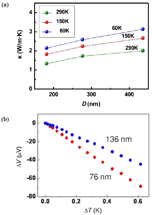
![Diameter-dependent thermal conductivity of individual PbTe nanowires. The temperatures are 60 150 and 290 K respectively. TEPs(S) of -130 and -76 μV K-1 are obtained from the slope of a linear fit to the data at 300 K. Reproduced with permission from [37].](http://oak.go.kr/repository/journal/11441/E1TEAO_2011_v12n6_227_f003.jpg)
![(a) Resistivity and (b) thermopower as a function of NW diam-eter at 300 K. Inset shows a color-enhanced SEM image of a typical device. The dashed lines in (a) and (b) are bulk values. Reproduced with permission from [59].](http://oak.go.kr/repository/journal/11441/E1TEAO_2011_v12n6_227_f005.jpg)
![(a) SEM image of the suspended microdevice for measuring the thermal conductivity of individual Bi nanowires. (b) SEM image of an individual Bi nanowire placed between the heating membrane and sensing membrane. Reproduced with permission from [44].](http://oak.go.kr/repository/journal/11441/E1TEAO_2011_v12n6_227_f006.jpg)