Amorphous silicon thin film transistors (a-Si TFTs) are widely used for consumer electronics. It has been demonstrated to be useful for employ in solar cells and flexible displays. Organic thin film transistors are of significance for applications involving low-cost electronic devices such as radio-frequency identification tags, flexible displays, memory and sensors. However, the applications of these devices are limited as a result of their low mobility and light/moisture sensitivity due to intrinsic material properties.
Transparent conducting oxide (TCO) and oxide semiconductor films have been used in many applications as transparent electrode materials for flat panel display devices, touch panels, and solar cells [1]. ZTO may be an interesting material for upcoming TCOs and for oxide semiconductor development due to its wide band gap, low cost and non-toxicity. Until now most of oxide semiconductors for TFT application have been prepared by vacuum deposition process such as sputter, PLD and ALD [2-4].
In order to achieve flexible display, low temperature process of solution processed oxide thin-film transistor (TFT) is in high demand.Displays fabricated with plastic substrate have the advantage of flexible, thin, light, and non-fragile characteristics with printing process, the high possibility of low cost and large area. Printing processes applied to TFT fordisplay are mostly ink-jet, micro-contact, and roll printing such as offset and gravure with high speed through put process, which can dramatically reduce the process cost. Most of the current work has been focused on the development of solution-processable semiconductors. Other components such as solution-processable conductor and dielectric materials have not yet received much attention.
There have been only few works relating to solution-processed source and drain electrodes in TFT application. The gold nanoparticle ink for organic TFT painted through a stencil with brush to make organic TFT provided an average mobility of 0.09 ~ 0.15 cm2/V s [5]. There was only one report regarding screen printing source/drain of silver nanoparticle for oxide IGZO TFT [6]. However, there was no report on the application of screenprinting source and drain electrodes to the solution processed oxide TFT. As a first step to attain an all-printing processed oxide TFT, screen -printing source and drain were applied to a solution processed ZTO semiconductor for the first time.
A bottom-gate and top-contact solution processed ZTO TFT
was prepared. As an active layer, zinc acetate dehydrate and tin chloride were mixed in 2-ethoxyethanol to form a sol-gel solution mixture, 0.7 M with the same molar ratio of Zn and Sn. The solution was stabilized by the addition of ethylamine. The inkjet printing system (Ommijet Mini-100, Unijet) was used with an orifice size of 50 μm. After ink-jet on the 300 nm thick thermally grown silicon oxide gate insulator on the heavily doped silicon wafer, the films were then thermally annealed at the temperature of 500℃ for one hour. Nano-silver ink, 55% of solid contents and viscosity of 22,000 cPs, was screen printed on a active layer and then, thermally annealed with different conditions to make a channel of 1,500-μm width and 100-μm length. All current voltage (I-V) characterizations of the ZTO TFT were carried out with a semiconductor parameter analyzer (Keithley 4200) in the dark at room temperature.
Transistors for all-printing display require printing steps for each unit process. Mostly, spin coating was applied at the initial stage and pursuit to the final roll to roll printing for the ideal printing system. Compared to the conventional lithography process for the fabrication of oxide TFT such as spin-coating, exposure, development, deposition of source-drain and lift-off, total process steps by using printing method can be reduced to only two steps, printing and drying. Screen printing techniques are widely used in commercial production, but rarely used in printing electrodes for TFT. Usually, source and drain metals were not patterned by screen printing due to the difficulty in channel length control. Two different silver nano inks, [PS-07 (400 cps, 30 wt% of Ag) and PA-10 (22,000 cps, 55 wt% of Ag)], were tested to find out an optimal source and drain contact. Criteria such as screen processability, drying time, pattern-capability, adhesion to semiconductor and delamination are the key parameters. As a standard process, screen-printed silver pastes were dried at 150℃ for 10 min in air. The sheet resistances were 120 mΩ/□ for PS-07, and 75 mΩ/□ for PA-10, respectively. These values were acceptable and were correlated with the silver content in the pastes. The conductivity of silver paste depends on the processing parameters like thermal annealing and paste formulation.
Electrical properties of solution processed ZTO TFT with screen printed source and drain electrodes.
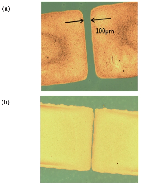
Screen printability was a key factor to define the channel. PS-07 was diffused to the outside of the designed area and could not make channel dimension due to the low viscosity of the paste. After many trials PA-10 was selected. Fig. 1(a) shows the microscopic image of source drain electrodes after screen printing of silver paste PA-10. Fine patterning channel layer of 100-μm of channel length was successfully defined by screen printing methodology. In the Lab, it was difficult to get such a clear channel dimension with screen printing technique. That is one of the reasons why most of the screen printed silver electrode was applied only to the gate electrode. As the adhesion of silver paste to active layer was not perfect, source and drain electrodes were easily delaminated. Sometimes it was brittle which dependedon the nano ink property.
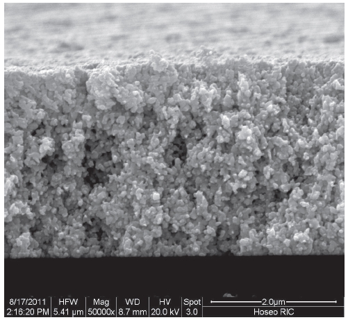
Fig. 2. shows the cross-sectional SEM image of the screen printed source and drain electrode. After thermal anneal, the silver nano particles of 50-nm shows well assembled and it interconnects with each other to form a good conductivity. Fig. 1(c) shows the cross-sectional view of silver S-D electrodes which were well mounted to a 4-μm thickness.
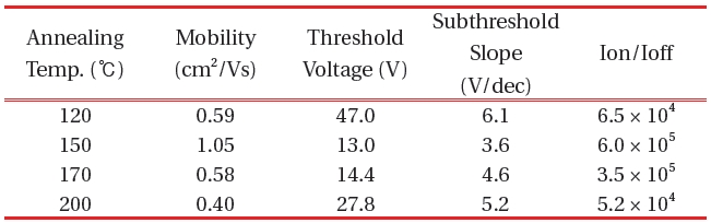
Sol-gel ZTO solution was spin-coated on the silicon oxide gate dielectric. The ZTO film was thermally annealed at 500℃ for about 1 hr. On the ZTO semiconductor, silver paste was screen printed and it was dried with different temperatures. Generally, silver paste makers recommended us to anneal the paste at a temperature of around 120℃ for 5 min. However, in the case of device fabrication this temperature does not always appear to be suitable for good property. When we prepared a solution of ZTO TFT with silver screen printed at different temperatures, the mobilities were 0.59 cm2/Vs for 120℃, 1.05 cm2/Vs for 150℃, 0.58 cm2/Vs for 170℃, and 0.40 cm2/Vs for 200℃, respectively. These values are of quite low property on comparison with other solution-processed ZTO with vacuum deposited on the source-drain electrodes as shown in Table 1.
In the case of vacuum annealing a temperature of about 120℃ was employed, the mobility slightly improved to 0.78 cm2/Vs. The reason may be due to the tighter contact with the ZTO semiconductor layer in vacuum, connection of silver paste together, and completely dries environment to remove moisture effects.
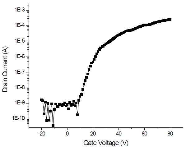
Figure 3 shows the transfer characteristics of the solution-processed ZTO TFT with a screen print source-drain at 150℃ in air. The drain current at the higher gate voltage was not smooth.
We tried more experiments on screen printed electrodes with ZTO, inkjet technology was employed. The piezoelectric inkjet printing system was used with a 50 μm orifice size. Uniform inkjet droplet ejection was achieved by applying a 60 V pulse at a frequency of 500 Hz with the substrate temperature of about 50℃ and a nozzle distance of 0.5 mm. After the inkjet printed on the silicon oxide gate insulator of the heavily doped silicon wafer, the films were then dried at 150℃ for 3 min to evaporate solvent. Then, it was thermally annealed at the 500℃ temperature for one hour. On the inkjet print ZTO, silver paste was screen printed to make source and drain electrodes.
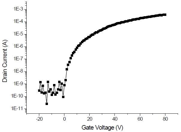
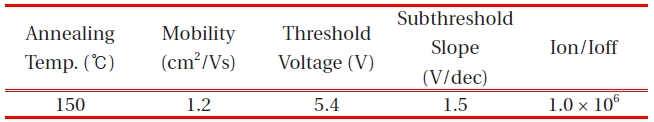
For the first time we successfully obtained the transfer characteristic of an inkjet-printed ZTO TFT with screen printed sourcedrain as shown in Fig. 4. The electrical properties were obtained as follows; a mobility of 1.20 cm2/Vs, a threshold voltage of 5.4 V,

Electrical properties of inkjet processed ZTO TFT with screen printed source and drain electrodes.
an Ion/Ioff current ratio of 106, and a subthreshold slope of 1.5 V/dec as summarized in Table 2. These properties are improved compared to the spin-coated solution processed ZTO TFTs. The inkjet ZTO area was not flat like the spin coated one. Droplets were overlayed and superimposed. In order to keep certain thickness, twice of ink jetting was necessary. Furthermore, the screen printing of silver nano paste on to the inkjet ZTO did not make good contact and so, sometimes delamination occurred during the fabrication process. The reason for improved electrical properties in inkjet ZTO TFT may be attributed to the physical anchoring between the ZTO droplet layer and the silver paste electrode, and the inkjet patterned ZTO active layer in the device.
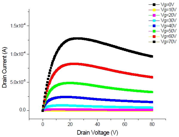
Figure 5 shows the drain current versus drain voltage (Id-Vd) output characteristics of the inkjet ZTO TFT with screen printing source-drain electrodes at various gate voltages. From the output characterization in Fig. 5, no crowding is observed, indicating a good contact resistance for the source-to-drain conduction. The output curves measured at Vd from 0 to 40 V, exhibit pinch-off and solid saturation, indicating that the device follows the standard field-effect transistor theory. The saturation slowly decreased with drain voltages especially at higher gate voltages due to the leakage current.
Screen-printed source and drain electrodes were successfully fabricated by silver nanoinks. The process condition was optimized. The electrodes were applied to the fabrication of a solution ZTO TFT and an inkjet ZTO TFT at the first time. The electrical property obtained by this technique was relatively good compared to other solution-processed ZTO TFT. More profound research should be performed in this particular area for further development and flexible electronic applications.