Photovoltaic energy industry and related technologies are expanding quickly and abruptly with increasing demand, necessitating the development of more effective solar cells. To aid in advanced research in solar energy technology, various characterizing tools such as scanning probe microscopy (SPM), Fourier transform infrared spectroscopy (FTIR), and Raman spectroscopy have been adapted. Recently, the technique of conductive atomic force microscopy (C-AFM), which is used to analyze the electrical property of nano-materials [1-6], has been modified to measure and characterize photoinduced current in various solar cells using light irradiation. We call such a system “a photoconductive AFM (PC-AFM).” The PC-AFM system can analyze the photovoltaic efficiency of solar cells in nanometer scale, and using this technology, it is possible to observe the phase separation, charge generation, charge transport, and charge collection phenomena, which occur in solar cell devices [7,8].
In this study, we designed and developed a poly-Si-based solar cell device using conventional Si processes such as phosphoryl chloride (POCl3) doping and diffusion methods. The photoinduced current was then observed using a PC-AFM system. During the PC-AFM analysis, we observed that the contact resistance between the cantilever tip and the sample surface can disturb the flow of photoinduced current. To reduce the contact resistance, the surface of the solar cell was coated with a thin film of Au (8 nm), and as a result, it was observed that the current flow behavior was significantly enhanced. In addition, to investigate the effect of the intensity of irradiation light used for inducing the current, we controlled the light intensity and scanned the topology and current-mapping images simultaneously with a PCAFM.
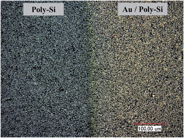
To investigate the light irradiation effect on the solar cell device using the PC-AFM, we prepared a p-n junction structured poly-Si wafer-based solar cell device. A 200 nm thick poly-Si wafer was heated in a diffusion furnace up to 850℃ with POCl3 to form a p-n junction on the surface of the wafer by the diffusion process. The thickness of the diffused n-type region is about 300 nm. After this process, the natural oxide layer was removed by rinsing with buffered HF solution. For verification of the contact resistance effect between the Pt-coated cantilever tip and the ntype Si surface, a thin Au (~8 nm) film was coated on the sample surface by a DC sputtering system with a patterned shadow mask. Figure 1 shows the optical microscope image of the Aucoated Si-solar cell surface. There is no difference in the topology of both the bare Si and the Au-coated area as the Au film is very thin. However, on analyzing using an optical microscope, we can distinguish a different color as shown in Fig. 1.
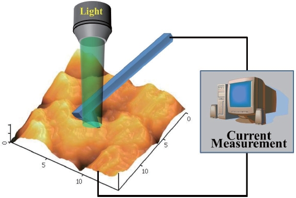
In this study, we used the E-sweep SPM model (Seiko Instruments, Inc.) that was interfaced with an external light source with controllable intensity to induce a photovoltaic phenomenon (Fig. 2).
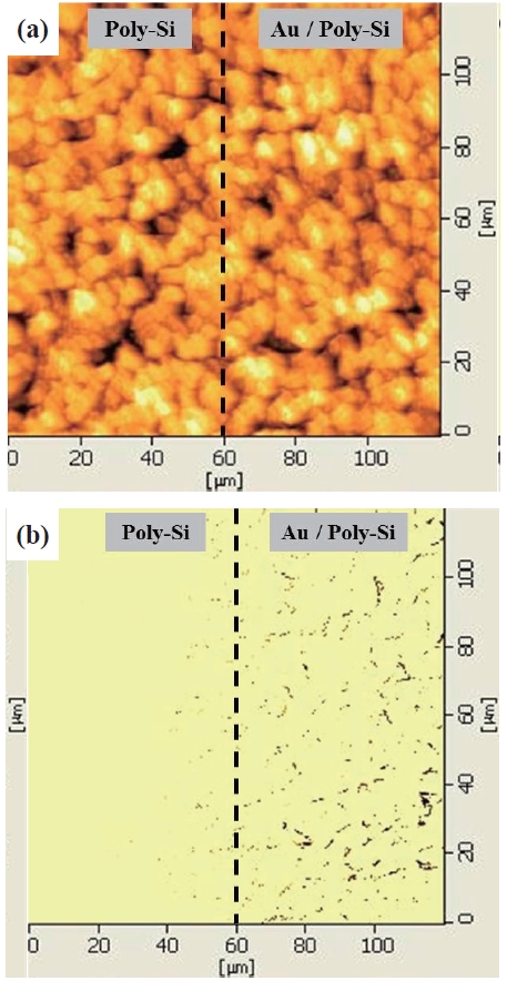
The Pt-coated Si cantilever tip with a spring constant of 3 N/m was used to measure the photoinduced current. First, a wide area (120 × 120 μm) scanning with 0 V bias was carried out in a dark box to verify the photovoltaic status of the solar cells without light. Next, the same area was scanned again with a 0 V bias
under the irradiation of light with intensity 80 W. The topology and current images were simultaneously obtained as shown in Fig. 3. In Figure 3(b), the dark area represents high conductance, and the bright area indicates low conductance.
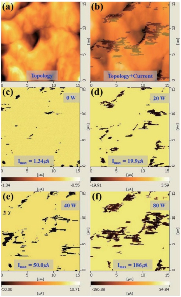
After the experiments, a small area (15 × 15 μm) scanning was carried out with 0 V bias under various light intensity conditions for a detailed analysis of the characterization of the correlation between light intensity and photoinduced current. During this process, the light intensity of the halogen lamp was varied from 0 to 100 W, and the topology and current images were simultaneously obtained. For the quantitative analysis of the electrical property of the photovoltaic effect, which was measured using the PC-AFM, the increasing maximum current level under each light condition was calculated, and the variation of the photoinduced current flowing area as a function of the light intensity was extracted.
The poly-Si-based solar cells were scanned using the PCAFM and the topology and current images were simultaneously obtained with 0 V DC bias, as shown in Fig. 3. In the currentmapping image, the dark area or spots indicate the flow of more vertical current through the cell surface when compared with the bright area. As the PC-AFM scanned both the bare poly-Si (Figs. 3(a) and 3(b), left half) and the Au thin-film-coated (Figs. 3(a) and 3(b), right half) surfaces, the difference in conducting properties of both the areas can be observed. As shown in Fig. 3(b), dark areas are found in the Au-coated image (Fig. 3(b), right
half) showing that the current flowed in this area, but no current passed through the bare poly-Si area (as shown in Fig. 3(b), left half).
The results indicate that high contact resistance, which originated because of the metal-semiconductor Schottky contact [9,10], exists between the Pt-coated tip and the poly-Si surface, and this disturbs the current flow in the case of the bare poly-Si surface. However, the contact resistance was remarkably decreased in the Au-coated area. As a result, we verified that the thin metal coating on the sample surface was very effective and necessary for the successful PC-AFM measurement.
From the current-mapping image, the good-conducting area was selected, and rescanned with a smaller scan area (15 × 15 μm) for a detailed analysis. The scanning of the selected area was carried out with a 0 V bias under various light intensity conditions for the characterization of the correlation between light intensity and photoinduced current. The light intensity of the halogen lamp used in the process was varied from 0 to 100 W in 20 W steps. Figure 4 shows the topology and current images with various light irradiation conditions. Figure 4(a) shows the analyzed topology image of the Au-coated surface. Figure 4(a) and the current image under the 80 W light condition (Fig. 4(f )) are overlaid to verify where the main current flowed and to verify the correlation between the topology and conducting area (Fig. 4(b)). From Fig. 4, we can see that photoinduced current shows a tendency to flow through the concave region of the texturized poly-Si for antireflection, and this phenomenon can be observed
in Fig. 3(b) as well. Such a result could be important information for the understanding of photovoltaic materials and their electrical properties.
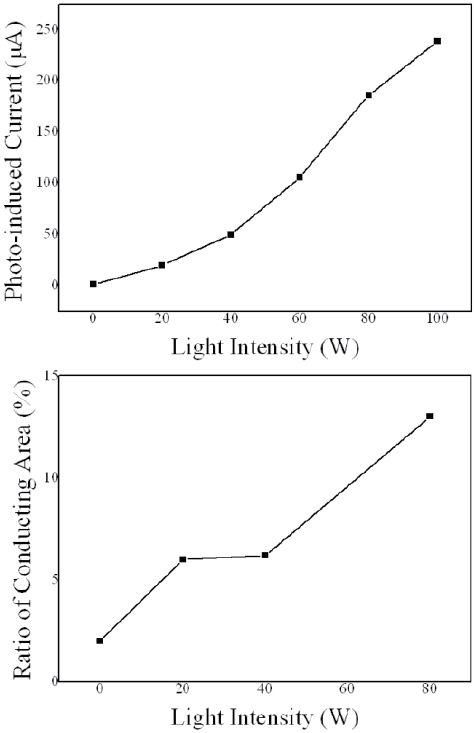
As the intensity of light becomes stronger, the maximum current value and conducting area (dark color) increase simultaneously. The maximum photoinduced current values were 19.9 μA, 58 μA, 106 μA, 186 μA, and 240 μA at light intensities of 20 W, 40 W, 60 W, 80 W, and 100 W, respectively. As the light intensity becomes stronger, the highest current value increases to ~200 μA at 80 W as more electrons and hole carriers are generated because of the photovoltaic effect (Fig. 5(a)). However, the rate of increase began to reduce at around 100 W, and it is expected to be saturated at light intensities more than this. Another important result is the ratio of the conducting area, which was calculated by dividing the current conducting area by the total scanned area at different conditions. The good-conducting dark area appeared in the current image of 0 W and expanded gradually as shown in Fig. 4(c)-4(f ).
For the quantitative analysis of this phenomenon, the ratio of carrier-generating area to the remaining region was calculated using the PC-AFM images. The ratio of the conducting area increases up to ~15% of the total scanned area, but it is expected that it will not increase beyond this because of the limitation of the carrier generation as well as the low-resistance preference of electrical conduction (Fig. 5(b)).
Moreover, in this study, we observed that photoinduced current was generated even in the dark condition (0 W) and deduced that such a current component comes from the photovoltaic effect caused by the laser (wavelength λ = 610 nm), which was used in the AFM system for sensing the cantilever movement.
In this study, we attempted to examine the photovoltaic effect in real-time measurement of photoinduced current in a poly-Sibased solar cell using the PC-AFM system. Normally, there exists a high contact resistance in a solar cell, which originates from the metal-semiconductor Schottky contact and disturbs the current flow. To solve this problem, an Au thin film was coated on the device surface, which successfully decreased the contact resistance. In the PC-AFM analysis, the conducting cantilever tip was brought in contact with the surface of the solar cell and light from a halogen lamp was irradiated on the contact tip region. The topology and photoinduced current-mapping images were obtained simultaneously, and both the highest current value and the ratio of conducting area increase as the intensity of light becomes stronger. The results of the characterization were very reasonable and reproducible. Through this study, we have demonstrated that the PC-AFM is a novel and effective tool to monitor and evaluate the property of solar energy-producing materials and devices. Moreover, further studies and future investigation using cross-sectional measurement and Kelvin force microscopy (KFM) analysis of charge carrier generation and behavior are planned for the detailed characterization of the solar cell [11,12].