Organic light-emitting diodes (OLEDs) generate light by a recombination process of electrons and holes that are injected from the electrodes to an emission layer. It is self-emissive and it has advantages such as high contrast, excellent viewing angle,fast response time, and etc. Moreover, it also has a potential application to a flexible display. For a low-voltage operation and a low-power consumption of the device, an efficient charge-injection from the electrodes to the charge-transport layer is needed. The injected electrons and holes should also be efficiently recombined in the emission layer.
Since Tang and VanSlyke reported on efficient organic lightemitting diodes [1], a number of researches have led to the enhancement of the efficiency and luminance of the device out of the various structures and materials. One method of improving the efficiency of the organic light-emitting diodes is by using the low work function metals such as Ca, Mg, and Li. Kido et al. reported on the enhancement of the current density and luminance of the organic light-emitting diodes by doping low work function metals of Li, Sr, and Sm on the electron-transport layer [2]. Hung et al. reported on the enhancement of current density and efficiency of the device by introducing a lithium fluoride (LiF) layer near cathode [3]. It was explained that the LiF layer helps in the electron injection from the cathode to the emission layer by the lowering of an electron-injection barrier height. Jabbour et al. researched on the electrical properties of organic light-emitting diodes depending on the thickness of LiF electron-injection layer [4]. They achieved an external quantum efficiency of 3.2 %and 3.0 % with Mg and Al cathodes, respectively.
Recently, the performance of the organic light-emitting diodes is being researched with the use of electron-injection layer of carbonate materials [5-7]. Wu et al. reported an advantage of electron-injection layer of cesium carbonate (Cs2CO3) by comparing the performance of the devices with a use of Cs2CO3 and LiF layer [7]. They investigated on the electronic structures and electroninjection mechanisms by using photoemission spectroscopy. Li et al. reported that the evaporated Cs2CO3 decomposes to metallic cesium during a thermal evaporation. The deposited Cs layer functions as an electron-injection layer [7]. There are not many works that reported on the role of lithium carbonate (Li2CO3) in organic light-emitting diodes. Recently, Kao et al. used another carbonate material of Li2CO3 as an electron-injection layer. They performed an X-ray and photoemission study to see a reaction mechanism between the electron-injection layer and the emission layer [8].
The lifetime of the organic light-emitting diodes is being researched as an organic material is weak to an exposure of moisture and oxygen. There are dark spot and thermal aging in the degradation mechanism of the device [9]. In order to reduce a dark spot, prevention of moisture and oxygen to the device is needed. In order to reduce thermal aging, an improvement of the interface at an organic/metal is needed.
In this paper, we focus on a new electron-injection layer of Li2CO3, which is not widely used in the organic light-emitting diodes. We present an efficiency and lifetime improvement of the organic light-emitting diodes with the use of Li2CO3 layer in the device structure of ITO/TPD (40 nm)/Alq3 (60 nm)/Li2CO3 (x nm)/Al (100 nm) by varying the Li2CO3 layer thickness.
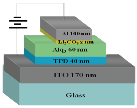
Devices were fabricated inside a vacuum chamber by thermal evaporation. Figure 1 shows the manufactured structure of ITO (170 nm)/TPD (40 nm)/Alq3 (60 nm)/Li2CO3 (x nm)/Al (100 nm) device. Here, Li2CO3 material was used as an electron-injection layer. The thickness of Li2CO3 layer varied from 0 to 3.3 nm. Figure 2 shows the molecular structure of Li2CO3 material. The molecular weight of this material is 73.89, a density is 2.110 g/cm3, and a boiling point is 1,310℃. Indium-tin-oxide (ITO) substrate
has a surface resistance of 10 Ω/sq. It was purchased from Samsung Cornings, and it was used as an anode.
An aluminum (Al) that has a purity of 99.99% was purchased from Aldrich Co. and it used as a cathode. N,N'-diphenyl-N,N'-di(m-tolyl)-benzidine (TPD) and tris(8-hydroxyquinoline) aluminium (Alq3) were used as a hole-transport layer and an emission layer, respectively. Thermal evaporation of the materials were performed at a pressure of 5×10⁻⁶ Torr. Deposition rates for TPD and Alq3, Li2CO3, and Al were 0.5~1.0 Å/s, 0.2 Å/s, and 0.5~5Å/s, respectively. The size of the substrate was 20×20 mm2, and the active area of the device was made to be 3×5 mm2.
Thickness of Li2CO3 layer was obtained from the quartz oscillator thickness monitor (STM-100/MF) which calibrated with density and geometric factors, and it was also measured using Alpha-Step 200 surface profiler. Current density-luminance-voltage characteristics of the devices were measured as a function of voltage using Keithley 236 source-measure unit, Keithley 617 electrometer, and Si photodiode at room temperature.
We have studied how the Li2CO3 electron-injection layer affects the performance of the organic light-emitting diodes. Electrical properties of the organic light-emitting diodes were studied depending on the thickness of Li2CO3 layer.
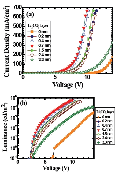
Figure 3 shows the (a) current density-voltage and (b) luminance-voltage characteristics of the ITO/TPD/Alq3/ Li2CO3/Al devices for various thicknesses of Li2CO3 layer that ranges from 0 to 3.3 nm. Figure 3(a) shows that the current density-voltage characteristics. In general, it shows a strong rectification behavior. General behavior in this figure is the following. As the thickness of Li2CO3 layer increases in the device, the voltagedependent current density of the device increases up to 0.7 nm thick Li2CO3 layer. Then it gradually decreases. For example, the current density at 8.0 V for the device with 0.7 nm thickness of Li2CO3 layer is increased by a factor of about 130 compared to the one for the device without the Li2CO3 layer. Figure 3(b) shows a corresponding voltage-dependent luminance of the same devices. In this figure, we can see that the use of Li2CO3 layer in the device causes an improvement in the luminance and turn-on voltage. The luminance of the device at 8.0 V with an insertion
of 0.7 nm thick Li2CO3 layer is about 3,000 times higher than the one without the Li2CO3 layer. There is also a dramatic reduction in the turn-on voltage of the device from 6 V to 2.5 V with the use of Li2CO3 layer compared to the one without the Li2CO3 layer. A thing to be pointed out is, irrespective of the Li2CO3 layer thicknesses that we have studied, the turn-on voltage of the device is almost the same.
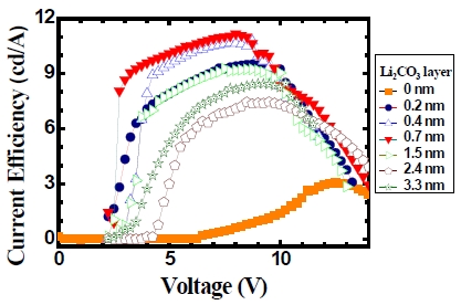
Figure 4 shows the corresponding current efficiency of the devices as a function of voltage obtained from the data of Fig. 3. In general, the efficiency of the devices is improved by employing the Li2CO3 layer to the device. And there is a shift of the voltage where the maximum current efficiency occurs as the Li2CO3 layer thickness in the device changes. While the maximum current efficiency for the Al-only device occurs near 12 V, the maximum efficiency for the device with 0.7 nm Li2CO3 layer occurs near 8 V. However, when the Li2CO3 layer’s thickness becomes 3.3 nm, the maximum efficiency occurs near 10 V. If the current efficiency of the device is compared under the same applied voltage, Fig. 4 shows that the current efficiency for Al-only device at 8.0 V is about 0.62 cd/A, and the one for the device with 0.7 nm Li2CO3 layer is about 11.2 cd/A. Therefore, with the use of a thin Li2CO3 layer there is an improvement in the efficiency by a factor of about 18 compared to the one for Al-only device.
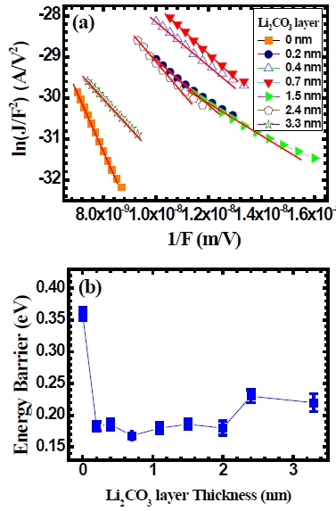
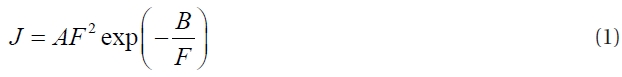
In order to understand reason for the improvement in the efficiency of the device with the use of Li2CO3 layer, a Fowler-Nordheim tunneling conduction mechanism model is applied to the current density-voltage characteristics. This is given by the following relation.
Here,
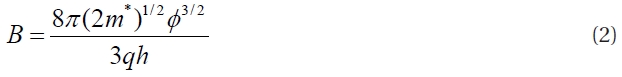
Here, Φ is an energy-barrier height,
In order to deduce an energy-barrier height at the interface of the device, a Fowler-Nordheim relation of ln (
the organic light-emitting diodes is calculated from the value of parameter
As the Li2CO3 layer thickness increases further, the energybarrier increases a little. From this result, we can speculate that the electron-injection energy barrier is affected by a Li2CO3 layer in the organic light-emitting diodes.
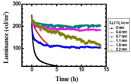
Figure 6 shows that the lifetime of the device depends on the thickness of Li2CO3 layer. When the thickness of Li2CO3 layer is 1.1 nm, the device shows a relatively longer lifetime. As the thickness of Li2CO3 layer increased further in the device, the lifetime of the device decreased. The improvement in the lifetime is thought to be due to the protection of the device from moisture and oxygen by using Li2CO3 layer.
Efficiency and lifetime improvement of the organic lightemitting diodes were studied by using an electron-injection layer of Li2CO3. The device was manufactured in a structure of ITO/TPD/Alq3/Li2CO3/Al by varying the thickness of Li2CO3 layer from 0 to 3.3 nm. The current density, luminance, and current efficiency were measured as a function of voltage. For the device with a Li2CO3 layer thickness of 0.7 nm, the current efficiency of the device at 8.0 V was increased to more than 18 times than the one without the Li2CO3 layer. An analysis using Fowler-Nordheim tunneling conduction mechanism shows that the barrier height for the device with 0.7 nm thick Li2CO3 layer is lower than the others. It is thought that the Li2CO3 layer-incorporated cathode in the organic light-emitting diodes which lowers the electron energy-barrier height between the cathode and the organic layer. Thus, the electron injection is improved and the recombination of the holes and the electrons is thought to be improved as well. When the thickness of Li2CO3 layer is 1.1 nm, the lifetime of the device was relatively superior to others. It is thought that the Li2CO3 layer in the device acts as a protection layer from oxygen and moisture.