Transparent conductive oxide (TCO) thin films such as In2O3, ZnO, SnO2 and In2O3: Sn (ITO) are technologically important due to their high optical transparency in the visible region, wide band gap and good electrical conductivity. Moreover, among them, indium oxide (In2O3) thin film is one of the most significant TCO materials. It finds its usage in diverse fields like: photovoltaic devices [1] transparent windows in liquid crystal displays [2] gas sensors [3-5] antireflection coatings [6] electro chromic devices [7] and solar cells [8]. Various investigations have been carried out on their growth conditions. Furthermore, studies on their properties with respect to the synthesis methods that are applied ranges across chemical vapor deposition [9], spray pyrolysis [10-12], vacuum evaporation [13] and magnetron sputtering [14,15]. Among these techniques, spray pyrolysis provides an easy route for the fabrication of thin films at a low cost. Moreover, it can be easily modified for mass production and device quality oxide films can be obtained over a large area.
In2O3 thin films are n-type semiconductors with wide energy band gap in the range of 3.60-3.72 (for several pyrolysis temperature, our results confirm these values but they are not reported here). The structure of In2O3 in its crystalline form is body centered cubic (bcc) with a lattice constant, a=10.11 Å [16].
In this study in order to study the structural, morphological, optical, electrical and gas sensing characteristics of spray pyrol-ysed In2O3 thin films which were prepared at different substrate temperatures, X-Ray diffraction (XRD), Scanning electron mi-croscopy (SEM), Atomic Force Microscopy (AFM), UV-Vis spec-troscopy, d.c electrical and gas sensitivity measurements were used. Most of the papers on gas sensitivity traits of In2O3 thin films are focused on the reduction of ambient (e.g. CO and H2) but there are fewer reports on ethanol sensitivity of spray pyrol-ysed In2O3 thin films. In this study, we have prepared such films and we have also investigated on their physical properties as well as gas sensing measurement.
Spray pyrolysis (SP) is basically a thermal reaction between a cluster of liquid / vapor atoms of different chemical species. It involves the spray of a solution, usually aqueous, in mist form and it contains solvable salts of the constituent atoms on, usually, a hot substrate. In the present study, nanocrystalline In2O3 thin films have been prepared on glass substrates (soda lime) by using SP. These films were prepared by spraying a water solution that contains indium chloride (0.2gr InCl3) onto glass substrate which is heated at different temperatures. Typical conditions for growth of In2O3 thin films by SP are as follows: distance between the spray nozzle and substrates 25 cm, carrier gas by using fil-tered compressed air, spray rate 19 lit/min, volume of solution, 40 ml. All the above mentioned parameters were maintained as a constant and only the substrate temperature was altered be-tween 400 and 600℃.
The structural properties were carried out by X-ray diffraction (PW1840) using Cu-Kα radiation having a wavelength of 1.5406 Å. The surface morphology was investigated by using a Scanning Electron Microscope (SEM) HITACHI S4160. Surface measure-ment was carried out using an atomic force microscopy (AFM) by NT-MDT equipment - SPM Solvers, PNL NTEGRA. Electrical resistivity, carrier concentration and Hall mobility were calcu-lated by the Van der Pauw method using PhysTech system. Opti-cal transmission for the samples was measured by using the UV-Visible spectrophotometer Cary 100.
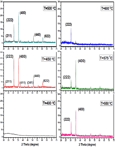
X-ray diffraction (XRD) patterns of the films as a function of substrate temperature are shown in Fig.1. The results show that the films which were deposited at a substrate temperature of 400℃ are amorphous in nature. With an increase in the substrate temperature, the crystallinity of the films improved and the relevant structure changed into polycrystalline type. The pre-ferred orientations are (400) and (222) respectively. By observing the characteristic peaks that appeared in XRD patterns we can confirm the cubic bixbyte structure of the prepared films [17]. According to Fig.1, the XRD intensity of the preferred growth orientation is highly dependent on the substrate temperature. The intensity ratio of the peaks (400) and (222) are similar at Ts= 450℃ and the (400) orientation increases along with the sub-strate temperature up to Ts=575℃. Beyond this temperature an abrupt decrease of the (400) orientation was observed with a corresponding increase in the (222) orientation.
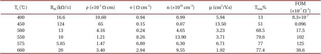
The mean crystallite size, D, was calculated for the diffraction peaks by using Scherer’s formula [18]. By increasing the substrate temperature from 575℃ to 600℃, the grain size decreased from 36.02 nm to 33.55 nm and this is in good agreement with the mo-bility data which is found in Table 1.
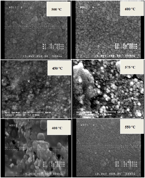
Figure 2 shows SEM images of In2O3 thin films that are pre-pared at different substrate temperatures. According to the SEM photographs, films deposited at 400℃ have a porous and uneven surface.
Results show that an increase in the substrate temperature highly affects the surface morphology and especially the grain di-mensions throughout the film. Deposition of films at lower tem-
peratures leads to an uneven surface morphology. On the other hand, increasing the substrate temperature caused improvement in the structure and the enhancement of the film uniformity.
According to the XRD spectra, films that were deposited below 400℃ are amorphous in structure but by increasing the substrate
temperature all the films exhibit a polycrystalline structure with (400) and (222) being the dominant orientations.
By increasing the substrate temperature from 400 to 500℃, the surface gets fully covered with fine and large grains. An in-crease in the grain size leads to a decrease in the density of the grain boundaries. As a result, there is enhancement in the car-rier concentration and the conductivity (Table 1) [19]. By further increase in the substrate temperature (550℃ to 600℃), the XRD spectrum exhibits better crystalline structure [20].
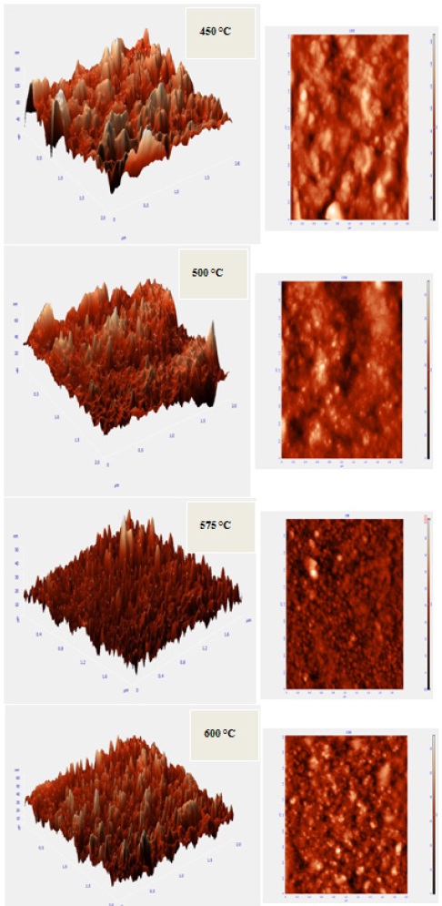
Typical AFM images of In2O3 films are deposited at various substrate temperatures and they are shown in Fig. 3. As shown in this figure, the substrate temperature greatly affects the surface morphology of the deposited films. Films that are deposited at lower temperature show a rough surface and poor quality while a further increase in the substrate temperature (575℃ to 600℃) leads to better surface quality and crystallographic structure. This is in close agreement with XRD & SEM observations.
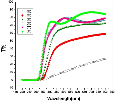
Figure 4 shows the optical transmittance curves as a function of wavelength for the In2O3 thin films that are deposited at vari-
ous substrate temperatures. Moreover, it can be observed that the optical transmittance of the films was also affected by the deposition temperature. The optical transmittance observed in the films changed from 13% to 77% with an increase in the depo-sition temperature. Furthermore, high transmittance in the films was attributed to less scattering effects, structural homogeneity and better crystallinity. A blue-shift in the absorption edge with substrate temperature was also observed. Usually, the blue-shift of the cut-off edge occurs due to the increase in the grain size and this increase, arises from heat treatment [21]. This may be attributed to the annihilation of the defect states in the gap or the strain release.
The electrical properties were determined by using room temperature Hall Effect measurements in the van der Pauw con-figuration [22]. The negative sign found in the Hall coefficient confirms the n-type conductivity [23].
The variation in the electrical properties as a function of the substrate temperature is given in Table 1. It can be easily found out that, the resistivity decreases totally with substrate tempera-ture .
An atypical behavior is evident in the case of Ts= 450℃ (sudden increase in the resistivity) and this may be assigned primarily to the poor quality of the surface and the high roughness value [24]. On the other hand, the carrier concentration reaches to a mini-mum value of 0.07×1018 cm-3 in this case. With regard to ρ= (
The optical transmittance and electrical conductivity are two important parameters and against these parameters, quality of the transparent conducting oxides is judged. Moreover, these two parameters are inversely proportional to each other. A method for correlating these properties in TCO films is through the "figure of merit" (FOM). This criterion is independent of the film thick-ness and it was proposed by G. Haack [26,27]:


Variation in the electrical properties of In2O3 films as a function of substrate temperature.
Where, T is maximum value of the optical transmission and Rsh is the electrical sheet resistance. According to Table 1, as we were looking for a layer with both high transparency and low re-sistivity, we used FOM for the selection of the optimized layer at substrate temperature Ts=575℃.
In this study, the gas sensing properties of the nano-sized In2O3 thin films which are deposited by spray pyrolysis technique have been investigated for ethanol. The sensitivity, (S) of the film is defined as the ratio between the surface resistance of the film in air (Ra) and gas (Rg):
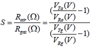
Where, VTa is source voltage in air, VRa is variant resistor voltage in air, VTg is source voltage in gas and VRg is variant resistor volt-age.
In the course of this present study we used the following val-ues for our experiments:

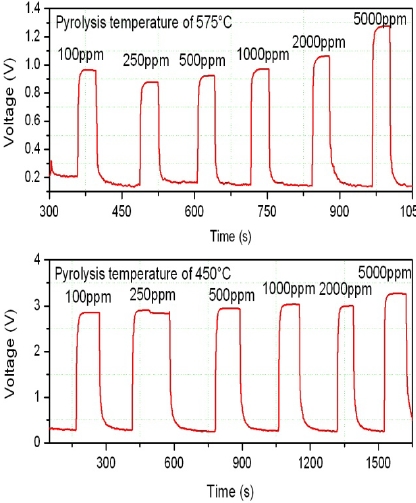
The dynamic response /recovery time cycle for the two
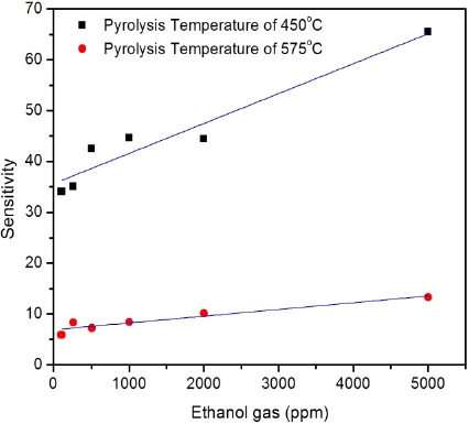
samples grown at 450 and 575℃ with several gas concentra-tions are shown in Fig. 5. It is obvious that the first sample (with the substrate temperature of 450℃) has higher sensitivity to the incoming gas and moreover, increasing the amount of gas leads to a higher response signal. Generally, it is accepted that a more resistive sample with higher roughness is better compared to an-other due to its better trapping situation for reducing the gases [28-30].
Gas sensing measurements of the films in ethanol with con-centrations of 100, 250, 500, 1,000, 2,000 and 5,000 ppm are shown in Fig. 6.
From Fig. 6 it is clear that the sensitivity of the sample which is grown at 450℃ is much higher compared to that grown at 575℃. Generally, films with higher sheet resistance possess a greater response to the reducing ambient (e.g. CO and H2) and a lower response to the ozone. This behavior indicates direct correlation between the gas response and the film stoichiometry [29].Gener-ally, when the conductivity (resistivity) is low (high), the response to the reducing gases is high [28]. According to XRD results (Fig. 1), the sample which is grown at 450℃ shows lower deviation of stoichiometry (higher Rsh~124 kΩ/□) compared to that grown at 575℃ (lower Rsh~6 kΩ/□). Hence, as expected, better sensitivity was observed for the sample grown at 450℃.
Thin films of In2O3 were deposited on glass substrates by spray pyrolysis technique at substrate temperatures that range be-tween 400-600℃. Results shows that the substrate temperature is one of the main process parameters and it has an important effect on the physical properties of the prepared films. Further-more, structural, morphological, optical and electrical properties of the films were studied and optimized conditions are achieved.
The X-ray diffraction studies revealed that the films which were formed at a substrate temperature of 400℃ were amor-phous while those formed at temperatures ≥450℃ were polycrys-talline. The SEM and AFM analysis revealed that at a substrate temperature of 575℃, the prepared films exhibited very smooth surfaces and good crystallographic structure. However, gas sens-ing analysis showed that the gas sensitivity is higher for the sam-ples grown at 450℃ that contains both higher surface roughness and electrical resistivity.