The reliability characteristics of ultrathin SiO2 film, which serves as the gate dielectric in silicon metal-oxide-semiconductor (MOS) devices, are one of the important issues to realize highly integrated devices. Deuterium incorporation compared with that of hydrogen at the Si/SiO2 area is known to improve device reliability [1]. The deuterium isotope effect is based on a much slower desorption rate of deuterium atoms from the Si/SiO2 interface. Deuterium has been incorporated into MOS devices by substituting deuterium gas for forming gas during post-metallization annealing under atmospheric pressure. This reduces hot-carrier injection (HCI) degradation in the MOS transistor by passivating the interface states at the Si/SiO2 interface. However, there is no consensus on the influence of deuterium incorporation on other degradations, such as negative bias temperature instability (NBTI) and stress-induced leakage current (SILC) [2,3].
For the integration of deuterium annealing into the mainstream with regards to semiconductor manufacturing, significant challenges still remain. When complementary-metal-oxidesemiconductor (CMOS) technologies incorporate multiple metals and dielectrics the improvement due to deuterium annealing was reduced further [4]. Deuterium diffusion takes place primarily through the silicon oxide (SiO2) in the MOS system due to the limited permeability of bulk Si, metal and even polysilicon to deuterium [5]. Deuterium implantation, on the other hand, can provide a spatially uniform distribution of deuterium throughout the gate oxide area [6]. Recently, deuterium implantation being carried out prior to the growth of gate oxide was reported [7]. However, it increased the silicon surface damage and the thickness of gate oxide compared with that of the control. In addition, the impact of deuterium implantation on device reliability, such as HCI and NBTI, has not yet been reported. The quality of gate oxide benefits from a deuterium isotope effect only when the deuterium is incorporated at the end of the process, in order to avoid desorption of the deuterium during hightemperature processing steps.
In this work, we report the reliability characteristics of MOSFET, including HCI and NBTI, when deuterium was incorporated in the gate oxide region by ion implantation after the first metallization. The implantation conditions for deuterium ion were calculated in advance through computer simulation (SRIM tool). Deuterium implantation is provided at low energy, and then subsequent post-annealing is achieved for the deuterium diffusion
into the gate oxide area.
MOS devices, p- and n-MOSFET, were fabricated using standard 0.18 μm CMOS technology for channel lengths down to 0.15 μm. The effective oxide thickness was in a range of 3 nm. The gate oxide film was produced with a conventional furnace in NO gas ambient. The deuterium implantation was performed at the back-end of the process line. The total thickness from the silicon surface to the top of the first metal was approximately 700 nm, including aluminum, silicon dioxide, and polysilicon layers. Post-annealing after implantation was achieved at 400℃ in N2 ambient for all devices in order to diffuse the injected ions and remove damages due to the implant process. The normal processed device (hydrogen furnace-annealed device) and the deuterium furnace-annealed device were also prepared to compare with the implant processed device.
Deuterium was implanted into our processed MOSFET with implantation energy of 30 keV and with a dose range of 1×10¹² - 1×10¹⁴ atoms/cm2. We found that the implantation with higher energy and more doses made the reliability worse and that with lower energy and fewer doses provided no deuterium effect within our device. The material stack of MOSFET in our wafer was composed of SiO2 [300 nm] / poly-Si [250 nm] / gate oxide [3 nm] / Si-substrate.
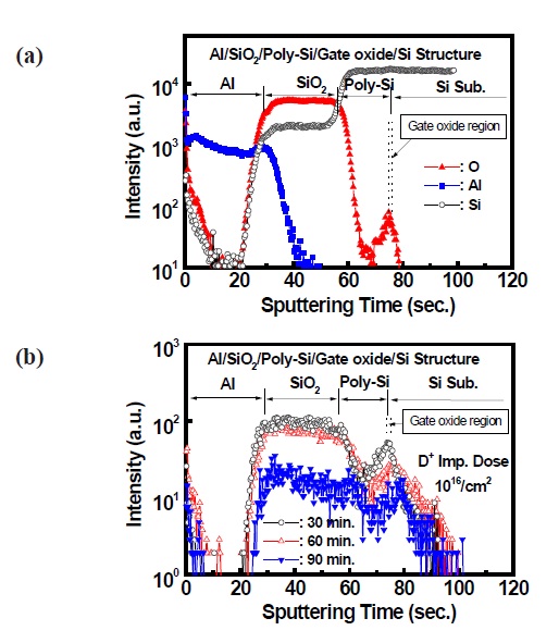
Secondary ion mass spectroscopy (SIMS) measurement for Al/SiO2/poly-Si/gate oxide/Si substrate which was implanted by deuterium on the top Al with 85 keV energy and 1016/cm2 dose is shown in Fig. 1. The aluminium layer covered the dielectric layers which solved the charging problem during ion sputtering for the depth profile. The implantation condition was chosen to make the peak of ion range localized in the middle of the polysilicon layer. From Fig. 1(a), each layer and its thickness above the
Si substrate were estimated and the thin gate oxide is assumed to be between the polysilicon and the Si substrate. Fig. 1(b) shows the depth profiles of deuterium depending on post-annealing time. The deuterium concentrations at the two SiO2 regions, including the gate oxide area, are higher than that in other layers when annealing time was 30 min. The implanted ions in the polysilicon layer diffuse toward the gate oxide area when postannealing is processing due to the chemical potential difference between SiO2 and Si [8]. Consequently, deuterium atoms are profiled in the 3 nm-thick gate oxides. The annealing time of 30 min. was observed to be an optimum time for post-annealing in our device structure.
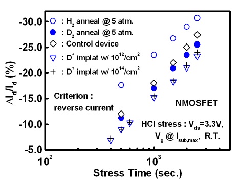
Passivation of dangling bonds at the Si/SiO2 interface can be evaluated by estimating the variation of drain current after HCI stress. Fig. 2 shows the decrease of reverse saturation drain current for devices processed with different deuterium incorporation methods as a function of HCI stress time. The results for the control device and the high-pressure hydrogen-annealed device are represented in order to compare them to that of the deuterium-implanted device. Deuterium annealing shows the suppression of HCI degradation that was already demonstrated by Hess [9]. He demonstrated the deuterium effect under the atmosphere (1 atm.) ambience of deuterium gas. We also found the same result, which was the suppression of drain current decrease under HCI stress. Therefore, the degradation curve for the 1 atm.-D2-annealed device could be positioned between that of the control device and that of the 5 atm.-D2-annealed device in Fig. 2. In the annealing process, the higher deuterium concentration is expected at the drain and source end of the channel due to the presence of sidewall spacers and a polysilicon layer above the channel area. That is, deuterium diffusion can have a localized effect. Deuterium-implanted devices have resulted in better suppression of degradation compared to annealed devices. The identical behavior regarding the current decrease was observed for 1×10¹² and 1×10¹⁴ atoms/cm2 implanted devices. In the implantation process, the depth at which concentration peak occurs was in the middle of the polysilicon area. Therefore, during subsequent N2 annealing deuterium has to diffuse to reach the interface along the channel. Only when deuterium with an optimum concentration is introduced will the oxide interface be more stable. When deuterium was implanted with more than 1×10¹⁴ atoms/cm2 HCI degradation was increased further even more so than the control device. In Fig. 3, we also found an isotope effect in the high-pressure hydrogen and deuterium anneal-
ing processes.
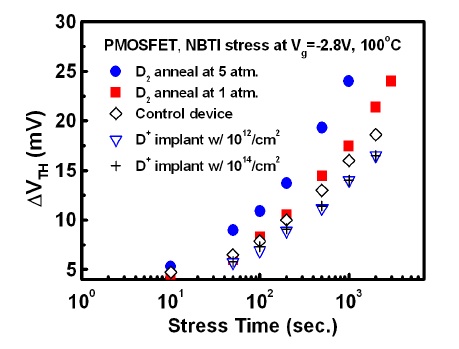
Figure 3 shows the shift of threshold voltage (VTH) for deuterium- incorporated p-MOSFET’s that were stressed by using NBTI condition. As for NBTI stress on MOSFET, both interfaceand bulk-reaction are possibly the reasons for the degradation. Therefore, NBTI degradation is commonly observed in the whole gate oxide area, which is in contrast with HCI degradation. In Fig. 3, the shift of VTH is suppressed in the deuterium-implanted device compared to the control device, and no improvement of VTH instability was observed in the deuterium-annealed device. During the annealing process, we found that NBTI was accelerated in a high-pressure ambience, which implies that surplus deuterium concentration in the gate oxide created more extrinsic defect in the oxide bulk and in the oxide interface near the drain and source sides. With regards to the hydrogen process we found the generation of defect clearly. A significant shift of VTH was found in the high-pressure (5 atm.) hydrogen-annealed device under the same NBTI condition, which implies that oxide-fixed charge is more easily generated at the high-hydrogenated device. The generation of extrinsic defect related with deuterium annealing has been reported by our group [10]. In the implantation process, deuterium can be spread into the gate oxide bulk through the optimum dose and energy. The NBTI condition leads to uniform donor-like interface trap generation in gate oxide interface of p- MOSFET and then injects channel holes into the gate oxide [11]. However, we have found that the effect of deuterium treatment was not shown at the gate oxide interface in p-MOSFET under the inversion bias mode [10]. Therefore, the suppression of NBTI degradation by deuterium implantation is attributed to the enhancement of gate oxide bulk quality.
Under the NBTI stress condition the channel holes can tunnel toward the thin gate oxide, and potentially gain the energy to break the Si-H(D) bonds inside the gate oxide. Based on such a degradation scenario, the deuterium effect shown in Fig. 3 is due to the bulk-reaction, not the interface-reaction. For application in the CMOS process, deuterium annealing is a convenient process to improve the interface property of gate oxide. However, deuterium implantation has an advantage for enhancing the oxide bulk quality and the interface property concurrently by the optimum implantation condition.
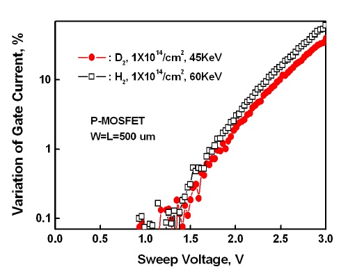
The stress-induced leakage current (SILC) under Fowler- Nordheim (FN) stress can be used to estimate the trap creation in the bulk of gate oxide. Fig. 4 represents the variation of gate current for deuterium-implanted p-MOSFETs, and its value was compared with that of the hydrogen-implanted device. The ion range of hydrogen implantation was adjusted to the same level of deuterium implantation. The current was measured at the gate terminal while the gate voltage was being swept from 0 to 3
V after finishing the constant voltage stress (Vg=-3.5 V). The device with deuterium implantation showed a lower gate leakage current for the entire range of sweeping voltages. The generation of stress-related bulk-oxide traps, which is a cause for leakage current, is suppressed through the incorporation of deuterium. We can then infer that the isotope effect is valid in our suggested implantation method. Therefore, deuterium implantation could be used to improve reliability, if a suitable implant condition is obtained.
We have demonstrated that the incorporation of deuterium in the gate oxide using ion implantation in the back-end process is an effective means to improve oxide quality and may be a viable alternative to deuterium furnace annealing. Isotope effect between hydrogen-implanted and deuterium-implanted devices was also demonstrated. Deuterium implantation brings about a reliability enhancement by suppressing the HCI and NBTI degradations. The obtained results show that the oxide bulk and the oxide interface benefit from the implantation of deuterium by optimizing the ion range, the dose, the energy, and the following N2 annealing by adjusting annealing time. The deuterium isotope effect in MOS device appears only when oxide degradation is precipitated by energetic “hot” carriers. It means that the deuterium and the hydrogen bonds within the gate oxide interface are desorbed at the same rate by non-energetic channel carriers. Finally, we demonstrated the reliability enhancement for the deuterium- implanted device by explaining the interface reaction in HCI stress and the bulk reaction in NBTI stress, respectively.