검색 전체 메뉴
PDF
맨 위로
OA 학술지
Optical Constants and Dispersion Parameters of CdS Thin Film Prepared by Chemical Bath Deposition
  • 비영리 CC BY-NC
  • 비영리 CC BY-NC
ABSTRACT
Optical Constants and Dispersion Parameters of CdS Thin Film Prepared by Chemical Bath Deposition
KEYWORD
CdS thin films , Chemical bath deposition , Spectroscopic ellipsometry , Complex dielectric function , Refractive index , Extinction coefficient , Single-oscillator model
  • 1. INTRODUCTION

    There is considerable interest in cadmium sulphide (CdS) compound semiconductor for thin film devices in electronic and photovoltaic applications [1-6]. CdS thin films are prepared by sputtering [5,6], thermal evaporation [4,7,8], screen printing [8], spray pyrolysis [9], and chemical bath deposition (CBD) [1,2,8,10-12]. The CBD process is a simple and inexpensive technique to obtain homogeneous, adherent, and stoichiometric CdS thin films [10]. Nanocrystalline CdS thin films are grown on glass substrates by CBD, in a solution bath containing cadmium salt, thiourea, and complexing agent. Sulphur ions are supplied by the decomposition of thiourea in an alkaline solution, and cadmium ions are usually complexed by NH4OH [11].

    CdS thin films by CBD occur by the ion-by-ion process (condensation of Cd2+ and S2- ions on the substrate) or by the clusterby- cluster process (adsorption of colloidal particles of CdS on the substrate) [12-14]. Lincot and Ortega-Borges reported that CdS formation reaction proceeds via two consecutive steps, the formation of a dense compact inner layer, followed by the formation of a porous less adherent layer, and the inner layer growth mechanism corresponds to the ion-by-ion process [15]. CdS can exist in two crystalline modifications : the hexagonal (wurtzite) phase and the cubic (zincblende) phase [16]. The crystal structure of CBD CdS thin films is known as hexagonal, cubic, or mixed structure of hexagonal and cubic. Cardona et al. reported that the E1A and F1 peaks are absent in the reflection spectrum and in the imaginary part of the dielectric constant of cubic CdS [17].

    The optical constants are necessary to study optoelectronic devices that use semiconductor thin films. Spectroscopic ellipsometry (SE) is a useful and nondestructive tool to obtain the optical constants of thin films. The complex dielectric function, optical constants, and microstructure of thin films are studied from spectroscopic ellipsometry [6,9,10,18-21]. The optical constants of refractive index, extinction coefficient, normal-incidence reflectivity, and absorption coefficient in thin films are obtained using SE data of the complex dielectric function [18,19,22]. The dispersion of refractive index can be analyzed using the Wemple- DiDomenico single-oscillator model (W-D model) [23], in which the refractive index n in the low absorption region is expressed

    using the oscillator energy, dispersion energy, and photon energy.

    In this study, nanocrystalline CdS thin film was prepared on glass substrate by CBD, and dielectric function and optical constants were investigated using spectroscopic ellipsometry. The dispersion of the refractive index of CdS thin film was analyzed using the W-D model, and the dispersion parameters of oscillator energy and dispersion energy were obtained.

    2. EXPERIMENTAL

    CdS thin film was prepared on glass substrate by chemical bath deposition in an alkaline solution. The alkaline solution bath, containing cadmium sulphate, thiourea, and ammonium hydroxide, was maintained at 80℃, and the pH value of the aqueous solution was 10 [24]. The deposited CdS thin film was rinsed in deionized water, and cleaned ultrasonically. The complex dielectric function and microstructure of CdS thin film were investigated using a spectroscopic ellipsometer (M-2000D, J. A. Woollam Co. Inc., Lincoln, NE, USA) with rotating analyzer, in the photon energy range from 1.24 to 6.48 eV at room temperature. The ellipsometric parameters ψ and Δ at an incidence angle were measured at each wavelength λ, in the range from 45° to 75°, at angle intervals of 5°.

    A four-phase (ambient/roughened surface layer/thin film/ substrate) model was used to obtain the optical parameters. For the roughened surface layer of CdS thin film, the effective medium approximation (EMA) [9,10,18] was used. The CdS thin film of the four-phase model was considered as a layer of compact CdS. Then, the roughened surface layer was considered as a mixture of CdS particles and voids. The data fitting was performed to minimize the mean square error (MSE) between the measured and calculated parameters of ψ and Δ. From the fitting results of SE data, the thicknesses of the inner compact layer and the roughened surface layer of CdS thin film were 296 and 18 nm, respectively. By employing the EMA, the roughened surface layer was found to be a porous layer, with 48.7 % CdS particles and 51.3 % voids.

    3. RESULTS AND DISCUSSION

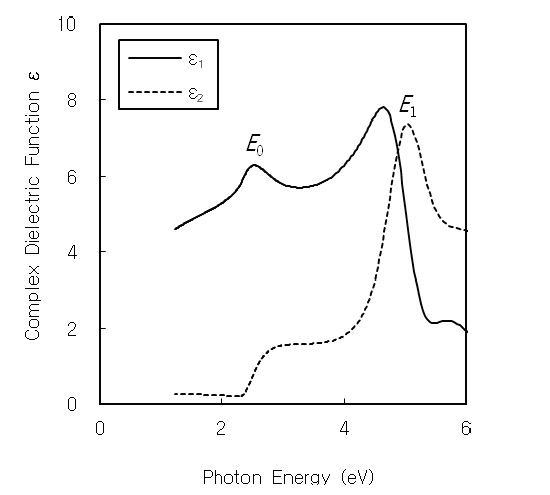
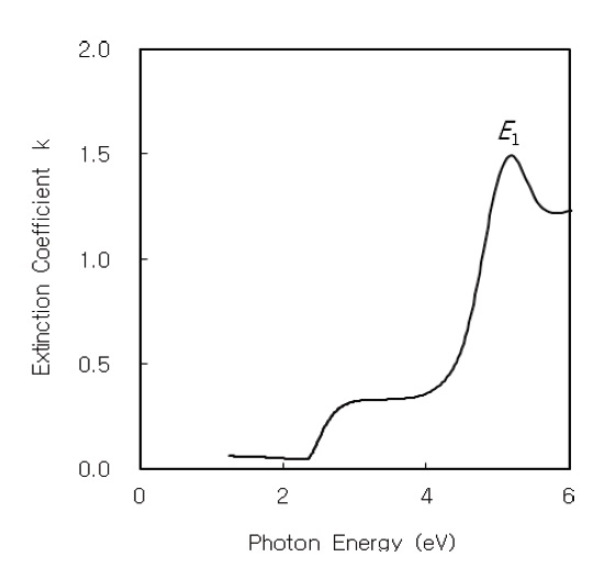
    The peaks in the dielectric function spectra are useful to study the interband transitions in the Brillouin zone. Cardona et al. reported that hexagonal CdS has the E0, E1A, E1B, E2, and F1 peaks in

    the imaginary part of the dielectric constant, and then the E1A and F 1 peaks are absent in cubic CdS. In other words, the hexagonal CdS has the E1A and E1Bdoublet peak, the cubic CdS has the E1B singlet peak [17]. On the other hand, the variation of the dielectric constant with photon energy indicates that some interactions between photons and electrons in the films are produced [25].

    The complex dielectric function ε(E)=ε1(E)+iε2(E) of CdS thin film is obtained by spectroscopic ellipsometry. Fig. 1 shows the real and imaginary parts of the complex dielectric function ε(E) of CdS thin film. Because there is the E1 singlet peak, the crystal structure of CBD CdS thin film is found to be cubic. From the complex dielectric function spectra of CdS thin film, two distinct structures are observed at E0 and E1 critical point energies. The peak E0 at 2.53 eV corresponds to the energy of transition from valence band to conduction band at the Γ point in the Brillouin zone. The peak E1 at 5.05 eV corresponds to the energy of transition along the L point in the Brillouin zone. It is known that the E0 and E1 critical points of cubic CdS are attributed to the Γ15v→ Γ1c and L3v→L1c transitions, respectively [26].

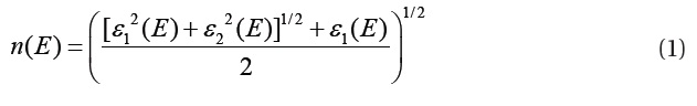
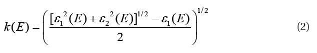
    The optical constants of the refractive index n and the extinction coefficient k are obtained from the SE data. The complex refractive index n*(E) is expressed by n*(E)=n(E)+ik(E). The refractive index n(E) and the extinction coefficient k(E) are numerically calculated from the complex dielectric function [22].

    image
    image

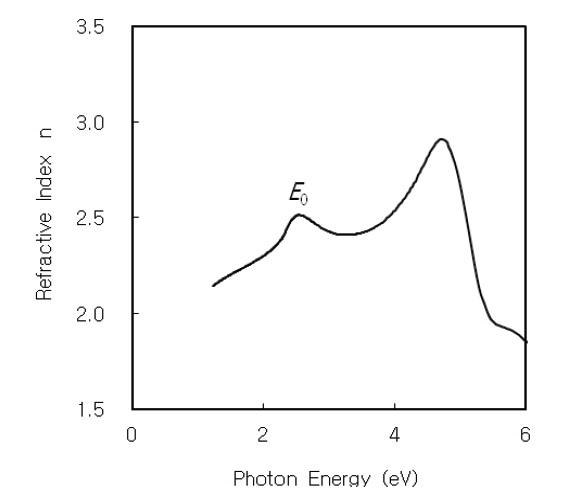
    Figures 2 and 3 show the refractive index n(E) and the extinction coefficient k(E) of CdS thin film, respectively. The n(E) and k(E) spectra reveal distinct E0 and E1 structures, corresponding to the interband transitions. As shown in Fig. 2, the E0 critical point of CdS thin film is observed at 2.55 eV. From Fig. 3 the E1 critical point of CdS thin film is observed at 5.18 eV.

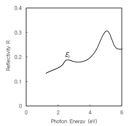
    The normal-incidence reflectivity R(E) and absorption coefficient α(E) are obtained using the refractive index n(E) and extinction coefficient k(E) [22].

    image
    image

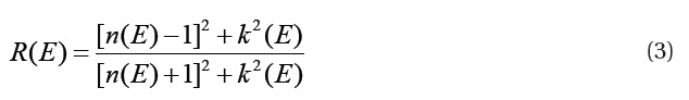
    Figures 4 and 5 show the normal-incidence reflectivity R(E) and absorption coefficient α(E) of CdS thin film, respectively. The R(E) and α(E) spectra reveal distinct E0 and E1 structures, corresponding to the interband transitions. As shown in Fig. 4, the E0 critical point of CdS thin film is observed at 2.60 eV. From Fig. 5, the E1 critical point of CdS thin film is observed at 5.22 eV.

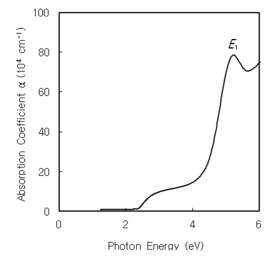
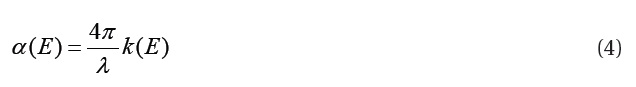
    The optical absorption coefficient α(
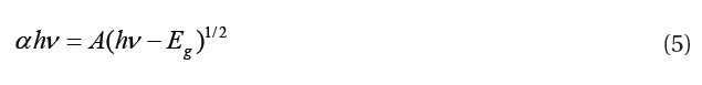
E) of CdS thin film can be obtained using the extinction coefficient k(E). For direct transition, the relation between the absorption coefficient α and incident photon energy can be written as

    image

    where A is a constant, and Eg is the energy band gap [27]. The optical band gap can be determined by extrapolating the straight line portion of the plot of (αhν)2 against to the energy axis. The optical band gap of CdS thin film was 2.78 eV, by extrapolating the straight line portion of (αhν)2 against the plot.

    The dispersion of refractive index below the interband absorption edge is analyzed using the W-D model [23]. In the W-D

    model, the refractive index
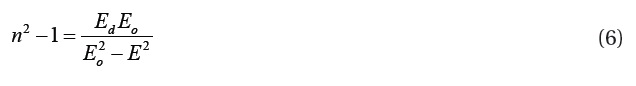
 n can be written

    image

    where E is the photon energy, Eo is the oscillator energy, and Ed is the dispersion energy. Wemple and DiDomenico reported that the dispersion energy may depend upon the charge distribution within each unit cell, and that it would be closely related to chemical bonding [23]. The oscillator energy Eo and dispersion energy Ed are obtained from the slope (EoEd)-1 and intercept Eo/Ed on the vertical axis of the straight line portion of (n2-1)-1 versus E 2 plot, respectively [28]. The static refractive index n(0) at zero photon energy is evaluated from Equation (6), i.e. n2(0)=1+Ed/Eo, and then the static dielectric constant εs is given as εs = n2(0) [23,29].

    Wemple and DiDomenico represented the dispersion energy Ed by the simple empirical relation

    image

    where NC is the coordination number of the cation nearestneighbor to the anion, Za is the formal chemical valency of the anion, Ne is the effective number of valence electrons per anion, and β is a constant β=0.26±0.04 eV for ionic materials, or β=0.37±0.05 eV for covalent materials [23].

    From the (n2-1)-1 versus E 2 plot of CdS thin film, the oscillator energy Eo and dispersion energy Ed were found to be 4.38 eV and 14.85 eV, respectively. The oscillator energy Eo was related empirically to the optical band gap Eg by Eo=1.58Eg . The dispersion energy Ed was related empirically to the optical band gap Eg by Ed =5.34Eg . The static refractive index n(0) and static dielectric constant εs were found to be 2.1 and 4.4, respectively. On the other hand, it was assumed that β=0.37 eV, Za=2, and Ne=8 for cubic CdS thin film, and the coordination number NC of the cation nearest-neighbor to the anion was calculated as 2.51.

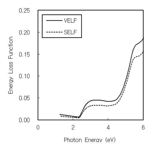
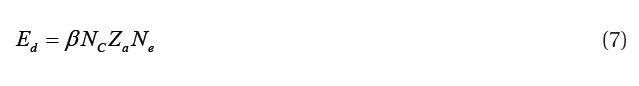
    The volume and surface energy loss functions are proportional to the characteristic energy loss of fast electrons traveling the bulk and surface of the material, respectively. The volume energy loss function (VELF) and surface energy loss function (SELF) are related to the real and imaginary parts of the complex dielectric function [30].

    image
    image

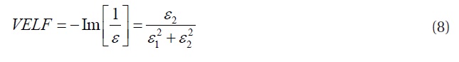
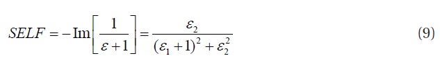
    Figure 6 shows the volume and surface energy loss functions of CdS thin film. The volume energy loss function is higher than the surface energy loss function. The energy loss functions reveal distinct Eo and E1 structures, corresponding to the interband transitions. Cardona et al. reported that in the volume energy loss function, the primary peak at 16.4 eV and the secondary peak at 11.8 eV correspond to plasma resonance of the valence electrons for cubic CdS [17].

    4. CONCLUSIONS

    CdS thin film was prepared on glass substrate by chemical bath deposition, and characterized by spectroscopic ellipsometry. To investigate the dielectric function and optical constants of CdS thin film, a spectroscopic ellipsometer with rotating analyzer was used. The crystal structure of CBD CdS thin film was found to be cubic, by the presence of the E1 singlet peak. The refractive index, extinction coefficient, normal-incidence reflectivity, and absorption coefficient of CdS thin film were investigated. The spectra of the dielectric function and optical constants of CdS thin film revealed two distinct structures at E1o and E1 critical points. From the spectra of the complex dielectric function, the Eo and E1 critical points of CdS thin film were observed at 2.53 and 5.05 eV, respectively. The dispersion of the refractive index of CdS thin film was analyzed by the Wemple-DiDomenico singleoscillator model. Dispersion parameters of the oscillator energy and dispersion energy of CdS thin film were investigated. Also, the volume and surface energy loss functions of CdS thin film were obtained using the real and imaginary parts of the complex dielectric function.

참고문헌
  • 1. Chang Y.-J, Munsee C. L, Herman G. S, Wager J. F, Mugdur P, Lee D.-H, Chang C.-H (2005) [Surf. Interface Anal.] Vol.37 P.398
  • 2. Ghosh P. K, Jana S, Maity U. N, Chattopadhyay K. K (2006) [Physica E] Vol.35 P.178
  • 3. Bhattacharya R. N, Ramanathan K, Gedvilas L, Keyes B (2005) [J. Phys. Chem. Solids] Vol.66 P.1862
  • 4. Abou-Ras D, Kostorz G, Romeo A, Rudmann D, Tiwari A. N (2005) [Thin Solid Films] Vol.480-481 P.118
  • 5. Romeo N, Bosio A, Tedeschi R, Romeo A, Canevari V (1999) [Sol. Energy Mater. Sol. Cells] Vol.58 P.209
  • 6. Podesta A, Armani N, Salviati G, Romeo N, Bosio A, Prato M (2006) [Thin Solid Films] Vol.511-512 P.448
  • 7. Singh V, Singh B. P, Sharma T. P, Tyagi R. C (2002) [Opt. Mater.] Vol.20 P.171
  • 8. Al Kuhaimi S. A (1998) [Vacuum] Vol.51 P.349
  • 9. Mathew S, Mukerjee P. S, Vijayakumar K. P (1995) [Thin Solid Films] Vol.254 P.278
  • 10. Sandoval-Paz M. G, Sotelo-Lerma M, Mendoza-Galvan A, Ramirez-Bon R (2007) [Thin Solid Films] Vol.515 P.3356
  • 11. Yu I, Isobe T, Senna M (1995) [Mater. Res. Bull] Vol.30 P.975
  • 12. Ortuno-Lopez M. B, Valenzuela-Jauregui J. J, Sotelo-Lerma M, Mendoza-Galvan A, Ramirez-Bon R (2003) [Thin Solid Films] Vol.429 P.34
  • 13. Sebastian P. J, Campos J, Nair P. K (1993) [Thin Solid Films] Vol.227 P.190
  • 14. Danaher W. J, Lyons L. E, Morris G. C (1985) [Sol. Energy Mater] Vol.12 P.137
  • 15. Lincot D, Ortega-Borges R (1992) [J. Electrochem. Soc.] Vol.139 P.1880
  • 16. Wenyi L, Xun C, Qiulong C, Zhibin Z (2005) [Mater. Lett.] Vol.59 P.1
  • 17. Cardona M, Weinstein M, Wolff G. A (1965) [Phys. Rev.] Vol.140 P.A 633
  • 18. Senthil K, Mangalaraj D, Narayandass Sa. K, Adachi S (2000) [Mater. Sci. Eng. B] Vol.78 P.53
  • 19. Sridharan M, Narayandass Sa. K, Mangalaraj D, Lee H. C (2002) [Cryst. Res. Technol.] Vol.37 P.964
  • 20. Qiu J.-H, Zhou P, Gao X.-Y, Yu J.-N, Wang S.-Y, Li J, Zheng Y.-X, Yang Y.-M, Song Q.-H, Chen L.-Y (2005) [J. Korean Phys. Soc.] Vol.46 P.S269
  • 21. Hu Z. G, Li Y. W, Zhu M, Zhu Z. Q, Chu J. H (2008) [Chu, Phys. Lett. A] Vol.372 P.4521
  • 22. Suzuki N, Adachi S (1996) [J. Appl. Phys.] Vol.79 P.2065
  • 23. Wemple S. H, DiDomenico M.Jr. (1971) [Phys. Rev. B] Vol.3 P.1338
  • 24. Park W.-D (2010) [Trans. Electr. Electron. Mater.] Vol.11 P.170
  • 25. Farag A. A. M, Yahia I. S (2010) [Opt. Commun.] Vol.283 P.4310
  • 26. Brus L (1986) [J. Phys. Chem.] Vol.90 P.2555
  • 27. Tauc J. C 1972 Optical Properties of Solids google
  • 28. Ilican S, Zor M, Caglar Y, Caglar M (2006) [Optica Applicata] Vol.36 P.29
  • 29. Qasrawi A. F (2007) [Opt. Mater.] Vol.29 P.1751
  • 30. Mahmoud S (1987) [J. Mater. Sci.] Vol.22 P.251
OAK XML 통계
이미지 / 테이블
  • [ Fig. 1. ]  Real and imaginary parts of the complex dielectric function ε(E) of CdS thin film.
    Real and imaginary parts of the complex dielectric function ε(E) of CdS thin film.
  • [ Fig. 2. ]  Refractive index n(E) of CdS thin film.
    Refractive index n(E) of CdS thin film.
  • [ Fig. 3. ]  Extinction coefficient k(E) of CdS thin film.
    Extinction coefficient k(E) of CdS thin film.
  • [ Fig. 4. ]  Normal-incidence reflectivity R(E) of CdS thin film.
    Normal-incidence reflectivity R(E) of CdS thin film.
  • [ Fig. 5. ]  Absorption coefficient α(E) of CdS thin film.
    Absorption coefficient α(E) of CdS thin film.
  • [ Fig. 6. ]  Volume and surface energy loss functions of CdS thin film.
    Volume and surface energy loss functions of CdS thin film.
(우)06579 서울시 서초구 반포대로 201(반포동)
Tel. 02-537-6389 | Fax. 02-590-0571 | 문의 : oak2014@korea.kr
Copyright(c) National Library of Korea. All rights reserved.