The information era has been enabled by systems design advances that result from the developments in circuits, materials and integration techniques. In the last few decades, electronic circuit developments have grown quickly since the transistor was developed in 1947. Such fast paced growth in turn places higher demand on low cost, small form factor, and lightweight circuit technologies for use in applications like wireless communication systems. Flexible lightweight designs have motivated the study regarding conducting polymers, discovered over 30 years ago, that have produced some basic building blocks like Organic Field Effect Transistors (OFETS) [1]. Another type of component that is important and highly desirable is the transparent interconnect for use between functional building blocks in hybrid integrated systems. Novel polymer materials offer promise and a first step in assessing its potential is to understand material properties by characterizing its dielectric constant and material loss.
The conducting polymer material used in this work is poly 3-hexylthiophene (P3HT), a solution composed of P3HT of 3 mg per chloroform of 1 ml. The material properties of P3HT are semiconducting and have been reported in the literature to have a field-effect carrier mobility of P3HT [2], a way to increase the mobility in P3HT [3]. P3HT is used as a semiconductor to create organic thin film transistors [4].When P3HT is heterojunctioned with n--Si to form diodes or with PCBM-71, photovoltaic devices [5] or organic solar cells [6] can be created. One of the attractive applications of the P3HT is flexible displays. It has advantages like offering spin coating capability and a low temperature process, but disadvantages such as a disordered structure and limited information for high frequency properties.
In this paper, the dielectric constant of P3HT is evaluated using the MIS capacitor method to characterize the high frequency behavior of an ultra-thin film for P3HT using the planar circuit design for high speed applications.
Two different methods are adopted in order to characterize the
P3HT film. The first method, MIS measurement, is performed in a low frequency band (1 kHz - 1 MHz). The second method, high frequency planar circuit measurement, is performed in a high frequency band (45 MHz - 50 GHz). By MIS measurement, the relative dielectric constant (εr) of P3HT film can be extracted. The εr value is very important to design a structure with P3HT in high frequency simulation software, where the extracted εr value of P3HT is required. Through the high frequency planar circuit measurement, the high frequency behavior of P3HT can be characterized. Also, the conductive behavior can be determined as a function of bias voltage (-20 V - +20 V) regarding the P3HT film operating in different modes. For example, the P3HT film operates in the accumulation mode and behaves as a lossy material when +20 V is applied.
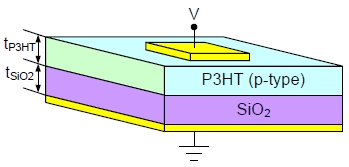
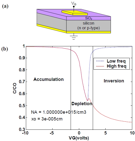
The first approach is a MIS capacitor method. The metaloxide- semiconductor (MOS) capacitor is a well-known structure. A structure of the conventional MOS capacitor is shown in Fig. 1(a). It consists of metal, silicon dioxide (SiO2), and a silicon semiconductor. A typical capacitance characteristic of the p-type semiconductor MOS capacitor is shown in Fig. 1(b). The capacitance of the MOS capacitor is normalized by SiO2 capacitance in the structure. Conventionally, high frequency means 1 MHz for this structure. There are three different regions depending on the bias condition, such as the accumulation, depletion, and inversion region. In the accumulation region, the total capacitance is just SiO2 capacitance and in the inversion region, the total capacitance is a series sum of SiO2 and semiconductor capacitance.
In order to extract the relative dielectric constant of the P3HT, a structure similar to the MOS capacitor is devised as shown in Fig. 2. For our structure, the stack-up of the MIS structure is upside down. For the insulator and semiconductor, SiO2 and P3HT are used in this work, respectively.
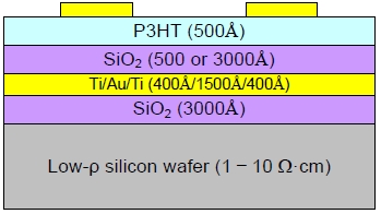
In MOS capacitor, the bias voltage is applied to SiO2, but in our MIS structure, the bias voltage is applied to the semiconductor. In this case, the accumulation region and the inversion region occur at the positive and negative bias voltage, respectively. The measurement results given in the next section will clearly show this phenomenon. The schematic shown in Fig. 3 describes the fabricated MIS structure for this work. In order to isolate the MIS
capacitor from the silicon wafer, SiO2 of 3,000 A is grown in a thermal furnace. For the ground plane of the MIS capacitor, titanium, gold and additional titanium are subsequently deposited on the 3,000 A thick SiO2. A layer of SiO2 for the insulator of the MIS capacitor is deposited by plasma enhanced chemical vapor deposition. Two different thicknesses (500 A and 3,000 A) of SiO2 film for the insulator are selected to investigate the effect of SiO2 thickness in regards to the MIS capacitor. Finally, P3HT is spincoated and another electrode to be applied to the bias voltage is deposited. The area of the electrode for the bias voltage on the P3HT film is 1 mm × 1 mm.
2.2 High frequency planar circuit method
The second approach is the high speed planar transmission line method to characterize the P3HT film in the high frequency regime. To this end, a planar transmission line needs to be fabricated on the P3HT film. A coplanar waveguide (CPW) is chosen as the planar transmission line. The CPW is easy to fabricate since a signal trace and a ground plane exist on the same plane. It can be used as a “sensor circuit” to analyze electromagnetic wave propagation at the presence of P3HT film.
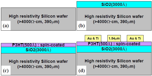
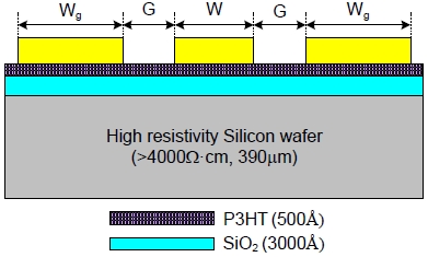
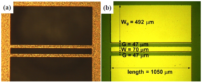
The schematic of CPW on P3HT film is shown in Fig. 4. The signal line width (W), gap between signal line and ground plane (G), and ground plane width (Wg = 3(W+2G)) are 70, 47, and 492 μm, respectively. The dimension of W and G provides us with the characteristic impedance of 50 Ω. To compare the performance of the CPW on P3HT film, a CPW on a bare silicon substrate and a CPW on 3,000 A thick SiO2 and silicon substrate are fabricated with the same dimension of W and G.
The fabrication process for the CPW on P3HT is depicted in Fig. 5. At first, 3,000 A thick SiO2 is grown in a thermal furnace. Then, P3HT film is spin-coated to be 500 A thick and cured in a vacuum chamber. After curing, the thickness of the P3HT film is
measured with an ellipsometer by 224.29 A. Since photolithography cannot be done with P3HT, a shadow mask made of 100 μm thick silicon wafer is used to define the area where the metal is deposited. After deposition of metal layers regarding titanium and gold in an E-beam evaporator, the shadow mask is removed and the CPW on P3HT film is fabricated. The metal thickness is 1.54 μm. A shadow mask and the fabricated CPW on P3HT are shown in Fig. 6 (a) and (b), respectively.
For the measurement of the MIS capacitor, a cryogenic vacuum probe station and an electrical measurement system (HP4280A: capacitance meter) are used. For the high frequency measurement, the HP8510C automatic network analyzer and Cascade Microtech on-wafer probe station with Cascade Air Coplanar GSG-150 probes are used to obtain two-port S-parameters. The thru-reflect-line calibration technique is used with MultiCal software [8] developed by the National Institute of Standards and Technology in order to remove probe contact effects from the measurement data.
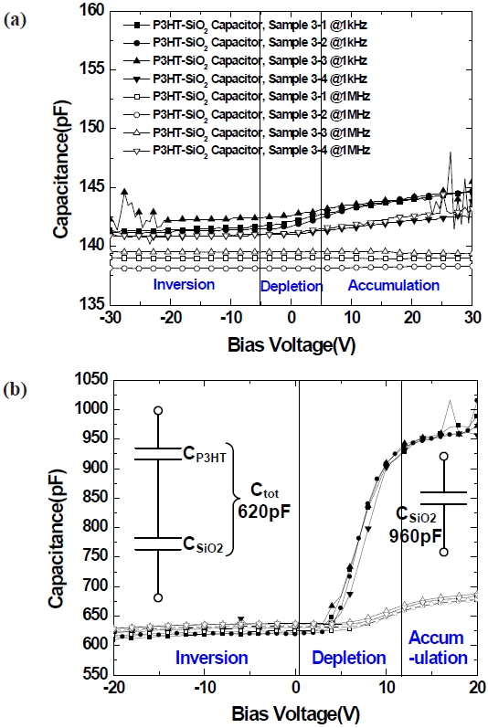
The measured capacitance of the MIS capacitor is shown in Fig. 8. As mentioned in Section 2, P3HT film is coated on two different thicknesses (500 A and 3,000 A) of SiO2 film. Fig. 7(a) and (b) show the capacitance with 3,000 A and 500 A thick SiO2, respectively. For the 3,000 A thick SiO2 film, the capacitance of the accumulation and inversion region is not quite different as shown in Fig. 7(a). The reason is because the capacitance of SiO2 film is much smaller than P3HT film due to the SiO2 film thickness. On the contrary, for the thin (500 A) SiO2 film, we can see the difference of capacitances between the accumulation and inversion region. In the accumulation region, the capacitance is 960 pF, which is only contributed by SiO2 film. In the inversion region, the total capacitance of 620 pF is a series sum of P3HT and SiO2 film. By simple calculation of the parallel plate capacitor given in
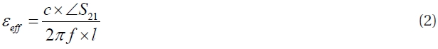
the equation (1), the relative dielectric constant of P3HT (εr,P3HT) can be estimated to be 4.4, which is a commonly accepted value for a polymer.
where ε0, A and d are 8.8542 × 10⁻¹² F/m, 1 mm2 and 224.29 A, respectively. It should be also noted that the accumulation and inversion region occur in the positive and negative bias voltage, respectively, which is reversed in position of the regions when compared to the conventional MOS capacitor characteristic shown in Fig. 1(b). The reason is because the bias voltage is applied to the semiconductor, P3HT in this work, instead of the insulator as in the conventional MOS capacitor.
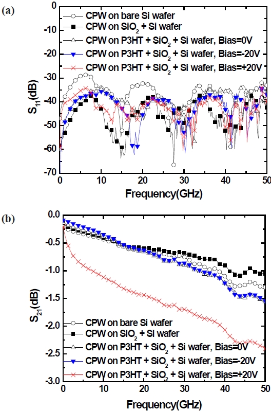
In order to investigate the behavior of the P3HT film in the high frequency regime, a CPW on the P3HT film is measured with various bias voltage conditions. The measured results are compared to the CPW on a bare silicon substrate and SiO2 film + silicon substrate as shown in Fig. 8. Since the characteristic impedance of the designed CPWs is 50 Ω, the return loss (S11) of each design is well below 20 dB as shown in Fig. 8(a). In order to analyze the bias dependent characteristics, various bias voltages from -20 V to +20 V are applied to the CPW on P3HT film. It is observed in Fig. 8 (a) that the bias voltages applied to the CPW on P3HT film barely affects the performance of S11. On the other hand, the insertion loss (S21) is affected when +20 V is applied to the CPW on P3HT film as shown in Fig. 8 (b). The performance of S21 clearly demonstrates that when positive bias voltage is applied to the CPW on P3HT film, the insertion loss becomes
worse. The CPW on P3HT film with +20 V is 1.5 dB lossier than the CPW on SiO2 film without P3HT film. The reason is because the P3HT film becomes conductive with positive bias voltage, which is consistent with the measurement results of the thick or thin film MIS capacitor with P3HT.
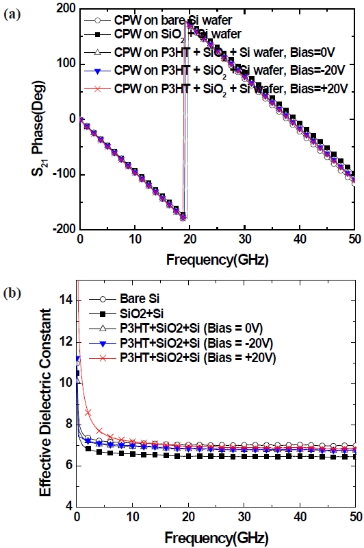
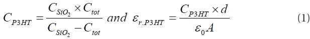
Figure 9 shows the phase response of the insertion loss. Distinguishing the characteristics among 5 different scenarios is not easy, however, when we extract the effective dielectric constant (εeff) from the phase response of the S21 using the equation (2), it is apparent that with positive bias voltage, the CPW on P3HT film is very dispersive around the low frequency band, which is a well-known characteristic for lossy substrates.
where
We have characterized the P3HT film with MIS capacitance measurements and high frequency planar transmission line measurements. From the MIS capacitance measurement, the relative dielectric constant of the P3HT film can be extracted and is around 4.4. In this technique, a thin insulator film is required due to the thin P3HT film. High frequency measurements detect the presence of P3HT film on the thick SiO2 insulator film. P3HT film operating in the accumulation mode produces an insertion loss increase by 1.5 dB at 50 GHz. Furthermore, P3HT film operating in the accumulation mode experiences higher dispersion at a low frequency band operation.

![(a) schematic of a conventional MOS capacitor and (b) its typical normalized capacitance characteristic [7].](http://oak.go.kr/repository/journal/11382/E1TEAO_2012_v13n5_237_f001.jpg)