Single-walled carbon nanotubes (SWCNTs) are one-dimensional carbon-based nanomaterials, and are considered a promising candidate for future electronic applications due to their unique electronic properties [1-6]. For instance, ballistic transport with high carrier mobility can be achieved. Notably, SWCNTs can carry high current density exceeding 109 A/cm2 [7]. Such excellent electrical properties stem from the relativistic nature of particles in SWCNTs similar to those in graphene [8,9], which can be thought of as an unrolled basic structure of a SWCNT. However, graphene is not suitable for application to field effect transistors, because it has only a zero band gap and the achievable on/off ratio is therefore little more than one order of magnitude. Recently, a high on/off ratio of 105 has been realized in a graphene-silicon Schottky barrier [10]. However, these barristors are not based on the intrinsic graphene properties, and thus it is not yet possible to realize the concept of “all carbon electronics”, which is often cited as a potential replacement for current silicon-based electronics [11]. On the other hand, SWCNTs exhibit either a semiconducting or metallic character depending on their chirality and, moreover, the band gap of semiconducting tubes can be tuned by controlling the chirality [3]. A high on/off ratio of the source-drain current through the field effect transistor devices using semiconducting SWCNT channels (more than 106) has been achieved [5,7,12,13]. Also, SWCNT crossed junction transistors with a very short channel length close to tube diameter have shown fast switching frequency of around 200 GHz [14,15]. Despite the excellent properties of SWCNTs as field effect transistor channel materials, it is not yet possible to obtain only semiconducting tubes from the growth stage. Instead, separation of the semiconducting tubes from bulk materials appears to be a more feasible route. Researchers have attempted to separate semiconducting SWCNTs by various approaches, such as centrifugationbased separation using the difference of the surfactant stabilization [16], repeated dielectrophoretic filtering [17], DNA-assisted separation [18], selective removal of metallic SWCNTs with small diameters by using nitric and sulfuric acid [19], and, very recently, single-chirality separation by gel chromatography [20]. Dielectrophoretic filtering is a chemical-free and nondestructive method, as the separation process is based only on the differences in the physical properties and dielectric constants of semiconducting and metallic tubes. However, the mechanism of the separation process is not yet clear. For instance, even in the region where the separation of electrodes is very large (~100 μm) compared to the tube length, the metallic tubes are captured by the applied ac electric field between the electrodes. This behavior cannot be explained solely by the dielectrophoretic force induced by an external electric field.
Here, we show that metallic SWCNTs aligned by dielectrophoresis are not deposited directly onto the substrate during the process but remain suspended in a solution due to the effect of pearl chain formation [21-24]. This was demonstrated by an optical microscopy study as well as by electrical measurements through the SWCNTs chains formed inside the solution.
2.1. SWCNTs solution in deuterium oxide
The sample was prepared by suspending SWCNTs in deuterium oxide containing 4 wt% of sodium dodecyl sulfate (SDS) as a surfactant. We used SWCNTs synthesized by a high pressure deposition carbon monoxide method in the experiment [25]. After 10 min of ultrasonic agitation, the sample was centrifuged at 50 000 g for 30 min and the upper 80% of the solution was carefully taken. The centrifugation process is required for extracting SWCNT bundles. The specific gravity of an individual SWCNT wrapped with SDS (SWCNT-SDS) is around 1.0 g/cm3 and that of a bundle of several SWCNTs wrapped with SDS (bundle- SDS) is around 1.2 g/cm3. Deuterium oxide was used instead of hydrogen oxide for better extraction of bundles because it has a specific gravity (1.1 g/cm3) larger than that of SWCNT-SDS and smaller than that of bundle-SDS [26]. The taken suspension showed no aggregation for more than a week.
2.2. Electrodes structure for dielectrophoresis
Wheel-type electrode structures were fabricated on top of a Si chip covered with a 500 nm thick thermal oxide using electron beam lithography and electron beam evaporation of Ti/Au (5 nm/100 nm). Here, Ti serves as an adhesion layer. The electrode configuration is the same as that used in Lee et al. [17]. The electric field applied to the electrodes generates not only a vertical gradient but also a horizontal gradient of the electric field. This chip was used for an in situ Raman measurements, which were performed while an ac electric field was applied. Another type of electrode structure with a two-probe configuration was fabricated by the same procedure. The width of the gap was 35 μm and the distance between the electrodes was 6 μm. The electrodes were used for electrical measurements through the SWCNT chain.
Raman spectroscopy was used to determine the metallic and semiconducting SWCNTs contents in a solution depending on the strength of the applied electric field [17,27]. An Ar+ ion laser with a wavelength of 514.5 nm (excitation energy of 2.41 eV) was used for the incident light source. The laser spot size was around 3 μm in diameter. Raman spectra were obtained either for the suspension in the deuterium oxide solution or for SWCNTs deposited on the SiO2 substrate after deuterium oxide was evaporated.
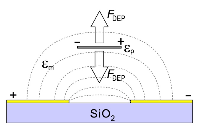
In a previous work [17], we extracted semiconducting SWCNTs in a hydrogen oxide solution using repeated dielectrophoretic filtering. A schematic illustration of the dielectrophoresis process is depicted in Fig. 1. When a uniform electric field is applied to SWCNTs suspended in a solution, the generated torque due to the dipole moment of the tubes aligns the SWCNTs in the direction of the applied field. The force is, however, balanced as long as the SWCNTs are not charged. No translational motion of the tubes is expected in this case. However, when the applied field is not uniform, the aligned SWCNTs that are suspended in the solution are attracted or repelled in the direction of the electrical field gradient. This dielectrophoretic force vector is given by [23,28],
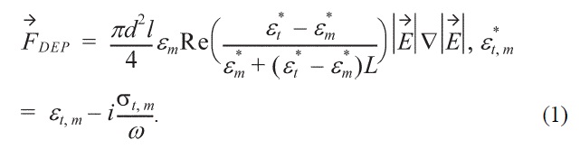
Here, d and l denote the diameter and the length of the tube, respectively,

is the external electric field,

is the com-
plex dielectric constant of a tube (medium), σ

is down to the substrate. The conductivity of the medium varies with the surfactant concentration. However, the conductivity and dielectric constant are many orders of magnitude larger than those of hydrogen oxide or deuterium oxide, even for high surfactant concentrations. The dielectric constant of hydrogen oxide or deuterium oxide can be assumed as εm ~ 80ε0, where ε0 is the dielectric constant of vacuum. According to Eq. (1), the sign of the dielectrophoretic force is always positive for any frequency [29]. Metallic SWCNTs are therefore pulled down to the substrate, where the electric field is the strongest. For semiconducting SWCNTs, which have a dielectric constant of εm ~2?5ε0 [29,30], the sign of the dielectrophoretic force is dependent on the frequency of the applied ac field as well as on the surfactant concentration. In our experiment conditions the dielectrophoretic force for semiconducting SWCNTs is negative and the SWCNTs remain in the solution [17].
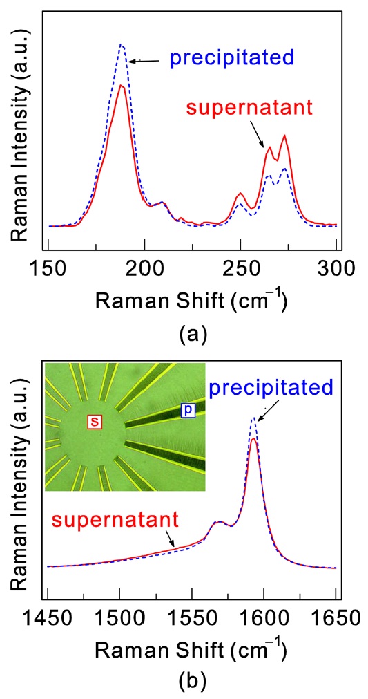
Fig. 2 shows the in situ Raman spectra around the radial breathing mode (RBM) and around the G mode for supernatant and precipitated SWCNTs. The spectra were obtained as follows. A small amount of the SWCNTs-deuterium oxide solution was dropped on top of the substrate with wheel-type electrode structures. An ac voltage with a peak-to-peak amplitude of 10 V at a frequency of 13 MHz was then applied between the wheeltype electrode pairs using a function generator. The inset of Fig. 2b shows an optical microscopy image taken during application of the electric field. Between the electrodes, SWCNTs are accumulated due to dielectrophoretic force. The Raman spectra were then obtained on the aligned SWCNTs between the electrodes (precipitated) and on the region where no electric field is applied, i.e. in the center of the wheel-type electrodes (supernatant). The regions are marked in the optical image. Generally, the RBM frequencies observed in a resonant Raman measurement are from only several species of the tube, the optical transition energy of which equals the incident laser energy [8]. According to the plot of the tube diameter versus the allowed optical transition energy, known as a “Kataura plot” [31], when using a 514.5 nm laser, the RBM peaks from semiconducting tubes appear at 130-200 cm-1 and the peaks from metallic tubes at 220- 280 cm-1. In our data shown in Fig. 2a, the peak at around 190 cm-1 represents semiconducting SWCNTs. The intensity of this peak in the spectrum obtained in the supernatant region is larger than the intensity obtained in the precipitated region. Metallic peaks in the range from 230 to 280 cm-1 are, on the other hand, larger in the precipitated region. These results imply that the ac electric field captures metallic SWCNTs between the electrodes, leaving semiconducting SWCNTs in the solution. The Raman G mode is a superposition of semiconducting and metallic tubes. Two sharp peaks from around 1560-1593 cm-1 are induced by semiconducting SWCNTs and a broad and asymmetric peak at around 1540 cm-1 is induced by the metallic SWCNTs [32,33]. In Fig. 2b, the slightly smaller intensity of the sharp semiconducting peak at around 1600 cm-1 for the precipitated region also shows the dielectrophoretic effect.
3.2. Dielectrophoretic filtering using deuterium oxide solution
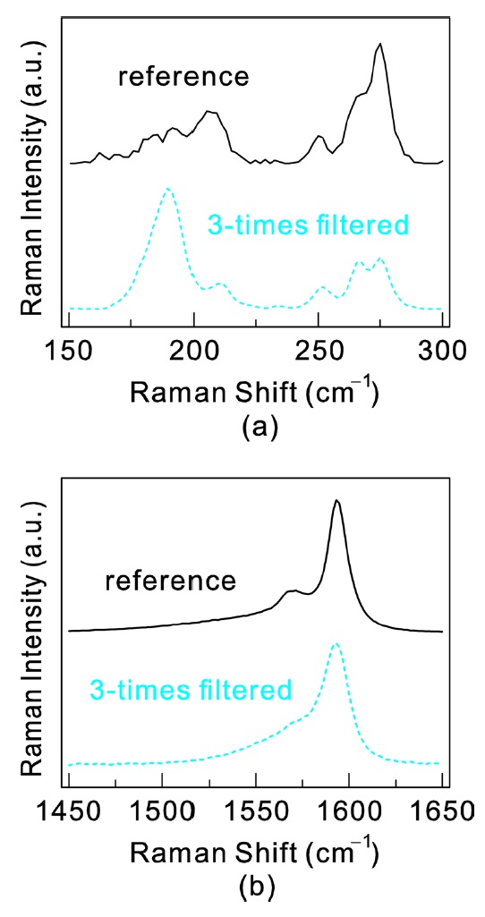
We performed dielectrophoretic filtering for the deuterium oxide solution. The details of the process are the same as in a previous work using a hydrogen oxide solution [17]. With the use of deuterium oxide as a solvent instead of hydrogen oxide the filtration efficiency was improved. Fig. 3 displays the Raman spectra on the initial deuterium oxide solution and the filtered sample. For this measurement, the SWCNTs were deposited on SiO2 substrates and the deuterium oxide was dried before the Raman measurements. The fraction of semiconducting SWCNTs among all the remaining SWCNTs in the filtered solution was estimated to be around 86% using an analysis of the peak intensity change. This shows that the filtration efficiency is significantly improved when using deuterium oxide, given that this level of semiconducting SWCNT content could only
be achieved with at least 3 repeated filtering steps when using a hydrogen oxide solution [17].
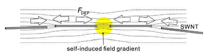
We note that the SWCNTs are accumulated even in the region where the distance between the electrodes is more than 100 μm. The behavior cannot be understood only by dielectrophoretic force, since the electrode spacing is much larger than the tube length and, moreover, the electric field is very small at this region compared to the field near the center of the chip. We also found that the aggregated SWCNTs between the electrodes dispersed into the solution again as soon as the electric field was turned off. These phenomena can be explained by a pearl chain formation [21-24]. A conceptual diagram of the pearl chain formation of the SWCNTs is shown in Fig. 4. In general, even under an external uniform electric field, the local electric field will bend near a dielectric particle. This self-induced nonuniform electric field near the particle will attract another dielectric particle by dielectrophoretic force, which occurs locally. As a result, the particles suspended in a solution will be linked to each other, forming a chain-like structure along the field lines. In our dielec-
trophoresis experiment, the tube-tube dielectrophoretic interaction may be stronger than the dielectrophoretic force induced by the external field gradient. The aligned tubes are therefore not deposited on the substrate but instead are suspended in the solution, thereby maintaining their chain formation.
3.4. Current-voltage characteristics through SWCNT chains
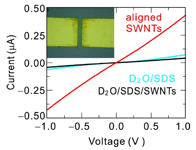
The pearl chain formation of aligned SWCNTs by the external electric field was demonstrated by an electrical measurement between the electrodes that had been used for the application of ac electric field. We fabricated simpler electrode structures with two wide electrodes, as shown in the inset of Fig. 5. The distance between the electrodes is 6 μm and the width of the electrodes is 35 μm. In the image, aligned tubes are visible since the image was obtained after the dielectrophoretic alignment. In order to maintain the SWCNT chains we put the chip into liquid nitrogen during application of the electric field. The deuterium oxide solution was then frozen immediately and the SWCNT chains were fixed in the solidified solution. The electric field was turned off before electrical measurements. At the liquid nitrogen temperature (around 77 K), we measured current-voltage (
We tested dielectrophoretic filtering for SWCNTs dispersed in a deuterium oxide solution. The results demonstrate that the deuterium oxide solution shows better efficiency for dielectrophoretic separation of semiconducting and metallic SWCNTs. We found that a large amount of the tubes aligned along the applied electric field are not deposited on the substrate but remained suspended in the deuterium oxide solution. The aggregation of aligned SWCNTs is released when the electric field is turned off. We suggest that the SWCNTs not only are aligned by the external electric field but also dielectrophoretically interact with the neighboring tubes due to the self-induced electric field gradient near the tubes. The SWCNTs are consequently attracted to each other, forming chain-like structures. A pearl chain formation of SWCNTs was demonstrated by electrical measurement through the chains of SWCNTs in liquid nitrogen.