Graphene has drawn intense research efforts since its first practical isolation was demonstrated in 2004 [1,2]. Its unique and novel material properties are expected to lead to many useful applications such as transparent conductive electrodes [3-5], nanoelectronics [6], and smart nanocomposites [7]. Since the electronic properties of graphene are highly sensitive to chemical interaction with its environments [1,8-10] owing to its peculiar electronic structure [11] and high surface/volume ratio, the understanding and manipulation of its chemical properties are essential in realizing such applications. Since graphene and graphite are highly inert against general chemical treatments, its chemical modification has resorted in harsh conditions such as oxidation at elevated temperatures [12], radical reactions [13-15], and strong mineral acids [16]. Although the previous approaches have their own strengths, some of them cannot be applied to certain applications due to their extreme conditions. In this regard, photo-induced chemical reactions can be beneficial since they require neither high temperatures nor strong acids. For instance, Liu et al. [17] have demonstrated that the crystalline structure of graphene can be modified by shining visible light with graphene immersed in an organic acid.
In the current study, we report that graphene exfoliated from crystalline graphite can be readily modified by oxygen atoms generated by UV photolysis of oxygen molecules. The introduced structural disorder was characterized by Raman spectroscopy [13,18]. We also found that the polymeric residues [19] originating from the adhesive tape used during the preparation of the graphene samples interfere with the oxygen-mediated photoreaction. The photoreaction was also successfully applied to large-scale graphene sheets grown by chemical vapor deposition (CVD) method.
Three sets of graphene samples were prepared on Si substrates covered with a thermally grown SiO2 layer of 285 nm thickness. All the substrates were thoroughly cleaned with piranha solution followed by rinsing with distilled water and drying under N2 blow. Graphene of the sample set A was prepared by the well-known micro-mechanical exfoliation of kish graphite (Covalent Materials Inc.). Although this method provides graphene samples of the best crystallinity, it also generates a significant amount of polymeric residues near the exfoliated graphene sheets since adhesive tape is used to exfoliate thin flakes onto the substrates. Sample set B was prepared by rubbing chunks of kish graphite against the substrates. While the yield of generated graphene sheets is very low, it does not leave any further contaminants on the substrates. Sample set C was prepared by transferring CVD-grown graphene onto the substrates according to the procedure described elsewhere [4].
For photoirradiation under a controlled gas environment, each of the samples was mounted in an optical flow cell with a 0.50 mm thick quartz window and an internal volume less than 100 mL. Either Ar or O2 gas (>99.999%) was introduced through the cell at a rate of 300 mL/min and the outgoing gas was made into bubble in a mineral oil. Photoirradiation was initiated after allowing the gases to flow through the cell for 20 min. The UV source, a pencil-type low pressure Hg lamp (Oriel, 6035), was operated at 10 mA in AC mode. Although its most intense spectral line is located at a wavelength of 254 nm [20], it also generates non-negligible emission at 185 nm that can photolyze O2 molecules into O atoms [21]. The distance between the lamp and the graphene sample surface was 7 ± 0.5 mm.
All the Raman spectra were obtained in a back scattering geometry using a 40x objective lens (NA = 0.60) in ambient conditions using a home-built micro-Raman setup, details of which were described elsewhere [19]. As excitation source, an Ar ion laser and an He-Ne laser, operated at wavelengths of 514.5 nm and 632.8 nm, respectively, were used. Spectral resolution values, defined by the line width of the Rayleigh scattering peak, were 11 and 3.5 cm-1 for the Ar and He-Ne laser excitation, respectively. The average laser power values were 1.7 and 4.3 mW for the Ar and He-Ne laser excitation, respectively.
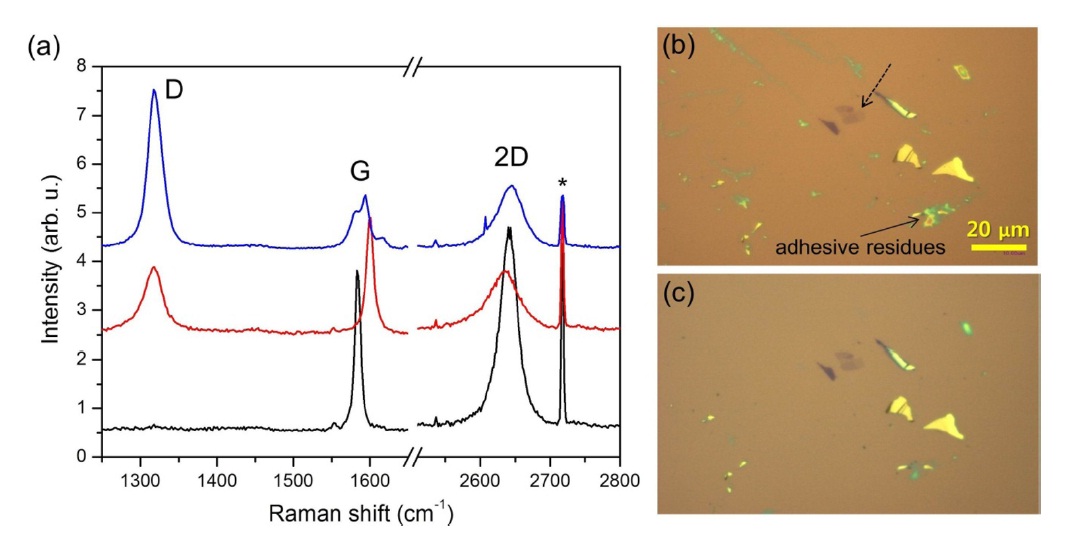
Fig. 1a shows the Raman spectra of the graphene (sample set A) before and after UV irradiation under O2 and Ar atmospheres. Disorder-related Raman D band was not observed at ~1320 cm-1 in the pristine graphene, indicating the high crystallinity of the sample. After the pristine graphene sample was mounted in the optical cell, oxygen gas was introduced through the cell. To generate oxygen atoms in situ, UV light from the Hg lamp was shone onto the sample for 45 min. The Raman spectrum (middle in Fig. 1a) obtained following the irradiation revealed a prominent D band, which indicates that the photoirradiation caused a significant number of defects on the basal plane of the graphene sheet [18]. To test whether the formation of the defects is directly related to the presence of O2, a similar run of experiment was carried out under Ar gas environment instead of O2. Surprisingly, the top spectrum in Fig. 1a obtained after UV irradiation for 45 min under Ar atmosphere shows an even larger D band. Since the Ar gas does not absorb light in the wavelength range of the Hg lamp’s emission, this suggests that a third body is involved in the photoreaction. The optical micrographs shown in Figs. 1b and c were taken before and after the photoirradiation in
the Ar gas flow. The yellow-greenish materials scattered around the thin graphene flakes in Fig. 1b are polymeric residues produced during the micro-mechanical exfoliation using adhesive tape [19]. Upon the UV irradiation under Ar atmosphere, the residues almost disappeared due to photodecomposition. This suggests a possibility that the formation of the D band caused by photoirradiation in Ar atmosphere relates with the presence of the polymeric materials.
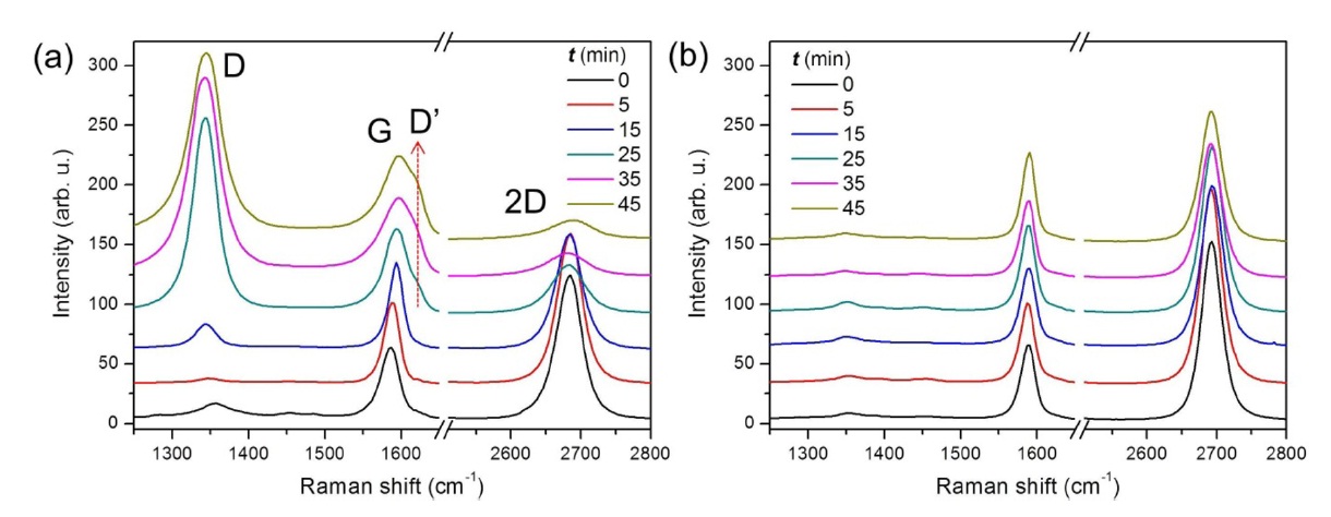
To investigate the role of the polymeric residues during the photoreaction, graphene sample set B was prepared from the same kish graphite as used for the sample set A but without using adhesive tape. Fig. 2a shows the series of Raman spectra obtained by varying the photoirradiation time (
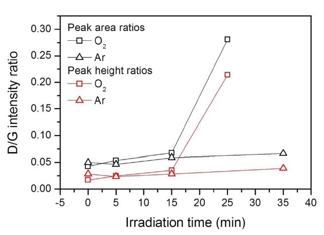
Fig. 2 indicates that the UV light itself does not cause chemical changes in graphene. In O2 atmosphere, the incoming UV light (λ ≥ 185 nm) photolyzes O2 molecules into reactive O atoms because the photodissociation threshold wavelength of O2 is 242.4 nm [21]. Since oxygen atoms are known to form epoxy groups on the perfect basal plane of graphite [22], the D band in Fig. 2a is attributed to epoxy functional groups on the graphene surface. The growth of the D band in the photoirradiated graphene under Ar atmosphere (Fig. 1a), however, can be attributed to reactive chemical species generated from the adhesive residues by the UV light, which is consistent with the UV-induced removal of the polymeric residues (Fig. 1c).
While the chemical nature of the UV-generated intermediates under Ar gas atmosphere is not known in the current study, recent reports on chemical reactions of graphene shed some light on the possible mechanisms. For example, hydrogen atoms are
known to form fairly stable C-H functional groups on the basal plane of grapheme [13,14]. Other radical species have also been found to undergo similar reactions [15,23,24]. Since the maximum photon energy of the employed UV light is beyond the photodissociation threshold for most organic polymers, it can be assumed that the photoirradiation generates various gaseous organic radicals that diffuse and attack the basal plane of the graphene sheets. However, the characterization of the surface functional groups on the graphene sheets is beyond the scope of the current study.
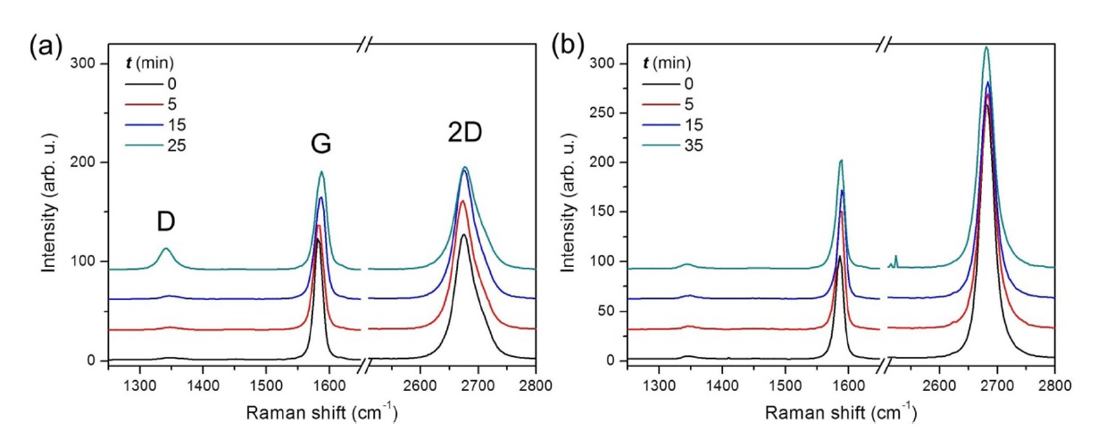
The practical applicability of the UV reaction was tested with CVD-grown graphene (sample set C), which holds promise as a material for large-area transparent conducting electrodes. Since the preparation of the samples includes polymer-supported transfer involving etching Cu foils, however, the resulting graphene transferred onto SiO2/Si substrates contains polymer residues and other contaminants [25]. Thus it is of importance to assess whether or not the inevitable surface contaminants interfere with the photoreactions. As shown in Fig. 4, the photoirradiation causes the D band to grow with graphene in O2 atmosphere, but
not in Ar. Thus, it is clear that the residues of the polymeric support, poly(methyl methacrylate), are not abundant or photoactive enough to interfere with the O atom reaction with graphene. It can also be seen that the rate of the reaction judged from the HD/HG ratios is larger for the CVD-grown graphene (Fig. 4a) than for the graphene exfoliated from kish graphite (Fig. 2a). This can be attributed to the fact that the CVD-grown graphene contains more structural disorders, ranging from atomic-scale defects to nanometer-scale ripples and folds created during growth and transfer [26], respectively. The chemical reactivity of graphene is considered to increase with the increase of the degree of its structural disorder [12].
The photoreactions of graphene demonstrated in the current study can be useful in manipulating the material properties of graphene. Most of all, the introduced defects are expected to reduce mechanical strength and increase friction on the graphene basal plane. As demonstrated in the hydrogenation reaction [14], it will be possible to modulate electrical conductivity by varying the photon fluence, and thus the density of defects. Owing to its high hydrophobicity, the basal plane of pristine graphene tends to avoid contact with hydrophilic materials. When terminated with proper functional groups, however, it can be possible to wet the graphene surface with materials of interest. Overall, the current method of manipulating the graphene surface photochemically will be found useful in various fields of research as well as applications.
We demonstrated that chemically inert graphene can be readily modified by oxygen atoms generated by a simple UVphotolysis of oxygen molecules. The epoxy functional groups formed by reaction with O atoms were characterized by Raman spectroscopy. It was also shown that the adhesive residues present in the graphene samples prepared by micro-mechanical exfoliation using adhesive tape strongly interfere with the UVinduced reaction. This makes it clear that attention needs to be paid when such residual contaminants can be activated to affect nearby graphene sheets. Finally, it was also verified that CVDgrown graphene can be modified by controlling the presence of O2 gas. This simple method can be readily carried out in ambient air and thus will be useful in chemical modification of graphene in the future.


![UV-induced changes in the Raman spectra of graphene exfoliated from kish graphite onto SiO2/Si substrates without using adhesive tape. The irradiation of UV light was carried out for a period (t) specified in the graphs with samples in (a) O2 and (b) Ar atmospheres. (λexc = 514 nm). The Raman spectra in (a) contain a small contribution from a nearby double-layer graphene because of the limited size of the single-layer graphene, which explains the line shape of 2D bands in (a). Nevertheless, the conclusion is not affected since chemical reactivity decreases with the increase of thickness [12] .](http://oak.go.kr/repository/journal/11010/HGTSB6_2012_v13n1_34_f002.jpg)