Carbon nanotubes (CNTs) have many exceptional properties that make them attractive for a variety of applications. Previous works have shown that CNTs have novel physical and chemical properties making them promising materials in field emission devices. In 1995, four years after the discovery of CNTs by Iijima [1], three groups reported field emission from CNTs at low turn-on fields and high current densities [2]. From 1998, the concept of using nanotubes in field emission devices spurred on efforts worldwide: a first display [3] as well as a lighting element [4] was presented. This area has been experiencing a rapid growth the past few years, and it is encouraging to note that two commercial products, namely high-brightness luminescent elements and an X-ray tube, have hit the market. Applications such as flat displays [4], X-ray tube sources [5, 6], electron sources for high-resolution electron beam instruments such as electron beam lithography machines and electron microscopes [7, 8] are under active consideration.
There are several properties of CNTs that make them extraordinary materials for field emission. Firstly, the graphene walls in them are parallel to the filament axis resulting in the nanotubes (whether metallic single-walled or multi-walled) exhibiting high electrical conductivity at room temperature. Secondly, CNTs are high in aspect ratio and whisker-like in shape. Utsumi [9] evaluated commonly used field emission tip shapes and concluded that the best field emission tip should be whisker-like, followed by the sharpened pyramid, hemi-spheroidal,and pyramidal shapes. It has been reported that even curly 'spaghetti-like' nanotubes stand up vertically like whiskers during emission under the application of an electric field [10]. Thirdly, CNTs can be very stable emitters, even at high tem-peratures. Previous researchers demonstrated that a multi-walled carbon nanotube (MWCNT) emitter could be heated up to 2000 K by its field-emitted current and remain stable. They claimed that this was the first reported observation of field emission in-duced stable heating. This characteristic is distinctively differ-ent from metal emitters. In metals, the resistance,
In general, single-walled carbon nanotubes (SWCNTs) have been studied to obtain low threshold electric field and high emission current density [12], but abrupt degradation of emis-sion current becomes a serious obstacle for field emission ap-plications. In contrast to SWCNTs, MWCNTs have shown bet-ter emission stability; however, a small field enhancement factor has been attributed to low emission current [13]. Recently, dou-ble-walled carbon nanotubes have been studied for this purpose due to high current density with long-term emission stability, but the poor production rate and following purification process of catalysts have been a serious bottleneck [14]. Few-walled car-bon nanotubes (FWCNTs), with small number of walls (2 to 6) and small diameters (below 5 nm), have been synthesized with high catalyst efficiency such that no further purification process was required [15]. Therefore, these FWCNTs could be the most promising candidates for the field emitter due to their intermedi-ate structural properties between SWCNTs and MWCNTs [16] and high production rate.
To fabricate CNT field emitters, there are several available methods including direct growth of CNT arrays using chemical vapor deposition (CVD), paste screen-printing of CNT powders, and electrophoretic deposition. However, each of them has sev-eral problems. The catalyst CVD method has to be performed at a higher temperature for CNT growth. Its fabricating process is limited by the scalability of the substrate size and it is diffi-cult to control CNT morphologies such as density and spacing. The paste screen-printing method, by contrast, is known as a more effective technology for large-scale production and has the advantage of a low cost process. However, substantial degrada-tion of emission tips caused by oxygen gases that are out-gassed from the organic vehicles in the paste cannot be avoided and as a result, poor uniformity of emission, poor emission spot density,and short lifetime will limit its application in commercial pro-duction. Furthermore, because the vapor from residual organic solvent will severely deteriorate the vacuum of field emission devices after the sealing process, a post-heat-treatment to re-move the residual organic solvent from the paste is necessary. The electrophoretic method has the problems of weak adhesion between CNT emitters and substrates, and non-uniformity in the thickness of the deposited layer, which will cause irregularity in the distribution of emission sites. The spray method is an easy and convenient method to deposit CNTs on the cathode sub-strates with a large area. However, the poor adhesion of CNTs to the substrate is also a serious drawback for long-term electron emission. Moreover, the spray method has been largely ham-pered by poor dispersion of CNTs, which was caused by their in-herent attractive van der Waals interactions between CNTs. One of the best methods to overcome this problem is to introduce carboxyl groups (-COOH) and hydroxyl groups (-OH) onto the surface of the CNTs through oxidation by nitric acid/sulfuric acid treatment. While this technique is a powerful method for improving the dispersion of CNTs, the acid treatment induces structural defects that change the property and morphology of CNTs.
In this study, we describe the fabrication of the CNT cath-odes by a spray method using a FWCNTs/binder one-compo-nent solution to improve the adhesion between the FWCNTs and the substrate for long-term emission stability. Moreover, various oxidation processes were applied to modify the sur-faces of pristine FW--CNTs. The hydration properties of FWCNTs and their effects on electron field emission property were studied.
The FWCNTs fabricated by CVD method were purchased from Hanwha Nanotech Co. We used a CNT product (CMP series) consisting of highly purified agglomerates of FW-CNTs with an outer mean diameter of 3 to 5 nm and a typical length ranging from hundreds of nanometers to a micrometer. Tetraethyl orthosilicate (TEOS) was purchased from Aldrich and used as received for improving adhesion between the FWCNTs and the substrate. Sulfuric acid (H2SO4) and nitric acid (HNO3) (Daejung Chemicals Co., Korea) were used for functionalization of CNTs on their side wall by chemical oxidation process. We used
2.2. Surface functionalization of FWCNTs
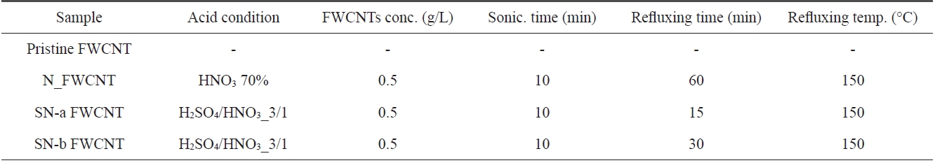
For the surface functionalization of FWCNTs, 50 mg of the agglomerated FWCNTs were mixed with 100 mL of one of the acid solutions listed in Table 1 by stirring for 5 min at room temperature and sonicating in a conventional ultrasonic bath (100 W) for 10 min; sonication longer than 10 min with high
[Table 1.] Acid treatment conditions for each sample

Acid treatment conditions for each sample
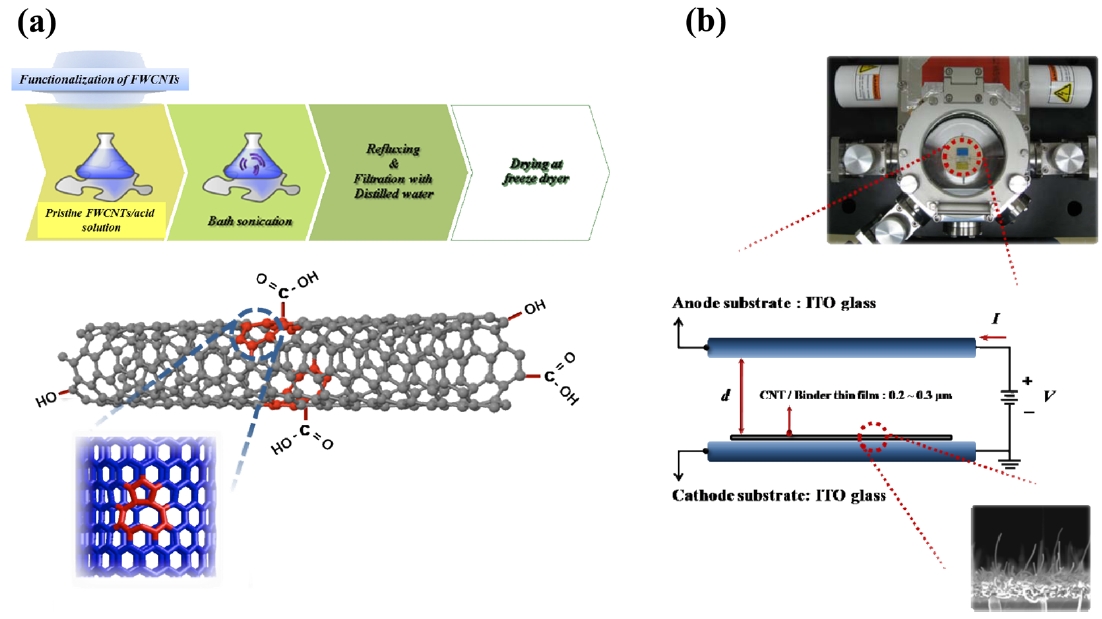
power could induce surface defects, not a functionalization, of FWCNTs. The sonicated FWCNTs/acid mixture was refluxed on a hot plate at 150℃ and then the slurry was filtered by vacuum filtration using an alumina filter and thoroughly washed with distilled water until the solution reached a pH value of 7. Fi-nally, the functionalized FWCNTs were dried by a freeze dryer for 48 h to remove moisture. Fig.1a describes the acid treatment process schematically.
2.3. Preparation of FWCNTs/TEOS sol onecomponent solution
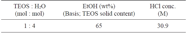
TEOS sol solution was prepared by mixing 5 g of tetrae-thoxy silane, 1.73 g of water, 3.33 g of ethanol, and 8 mg of 30.9 M hydrochloric acid, and performing a continuous sol-gel reaction at 60oC under 250 rpm (Table 2). After that,pristine and functionalized FWCNTs were dispersed in the DMF for 2 h in a conventional ultrasonic bath (100 W) at a definite concentration. Next, we centrifuged the solution 5000 rpm for 30 min to remove graphitic particles and large CNT bundles. Lastly, dispersed FWCNTs solution was mixed with TEOS sol and sonicated in a conventional ultrasonic bath (100 W) for 30 min (Table 3).
[Table 2.] Formulation of the TEOS sol

Formulation of the TEOS sol
[Table 3.] Formulation of the FWCNTs/TEOS one component solu-tion for spray coating
Formulation of the FWCNTs/TEOS one component solu-tion for spray coating
2.4. Preparation of FWCNTs/TEOS thin film field emitter
The field emitters using FWCNTs/TEOS one component solution were prepared by the following method. Firstly, the FWCNTs/TEOS one component solution was sprayed onto in-dium tin oxide (ITO) coated glass by an automatic spray coater (NVD-200, Fujimori, Japan) with a nozzle of 1.2 mm diameter at 135℃. The prepared FWCNTs/TEOS thin films (2 × 2 cm2)were then cured in a vacuum oven at 150℃ for 90 min. After thermal curing, they were found tightly adhered to the ITO glass. We performed the activation process by a taping method that creates many nanotubes aligned in the vertical direction.
To get information about functional groups on the nanotube surface, X-ray photoelectron spectroscopy (XPS) measurements were performed on a MultiLab2000 (Thermo VG Scientific, UK) with monochromatized Al Kα X-ray radiation as the X-ray source for excitation under ultrahigh vacuum system. The XPS core level spectra were analyzed with a fitting routine, which can decom-pose each spectrum into individual mixed Gaussian Lorentzian peaks. Raman spectroscopy (FRS-100S; Bruker, USA) with an Ar laser excitation of 633 nm wavelength was used to assess the quality of the graphitic structure of the FWCNTs. We measured the Raman spectrum from more than ten different points of each sample for correct information. The corresponding images of the samples were obtained by field-emission scanning electron mi-croscopy (FE-SEM, 10 kV, S-4800, Hitachi, Japan). The well-dispersed FWCNTs solution after centrifugation was analyzed by UV visible (UV-VIS) spectroscopy (cary 5000; Varian, USA) to determine the effect of acid treatment on the state of the disper-sion and dispersability of the nanotubes in DMF.
The field emission properties were measured in a diode type with a direct current bias inside a vacuum chamber un-der less than 5 × 10⁻⁷ Torr of pressure, as shown in Fig.1 b. ITO glass was used as an anode electrode separated by a 200μm polyethylene terephthalate (PET) spacer. To obtain stable field emission properties, an electrical aging process was per-formed by the following method: first, 100 repetitions of I-V sweeping up to 0.5 mA/cm2 of emission cur-rent density, then constant voltage annealing at 0.35 mA/cm2 of emission current density for 2 h.
During this electrical aging process, some protruded FW-CNTs were removed so that the length uniformity of FWCNT emitters was enhanced, which resulted in stable electron emis-sion. White phosphor-coated ITO glass as an anode was used to determine the emission pattern of FWCNT emitters.
3.1. Characterization of pristine and acid-treated FWCNTs
3.1.1. XPS analysis of FWCNTs
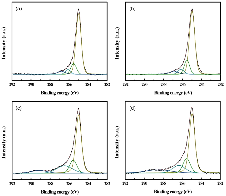
With reference to functionality grafting, XPS is a surface analytical technique that can provide useful information on the nature of functional groups and also on the presence of structural defects on the nanotube surface. The intensity
Relative percentage of functional components obtainedfrom curve fitting the C1s peak for the pristine FWCNT and oxidized FWCNTs
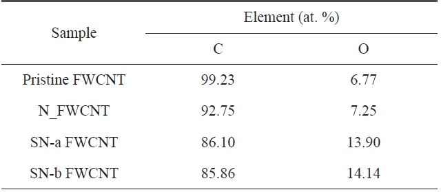
[Table 5.] Summary of the elemental composition for the pristine FWCNT and oxidized FWCNTs

Summary of the elemental composition for the pristine FWCNT and oxidized FWCNTs

where
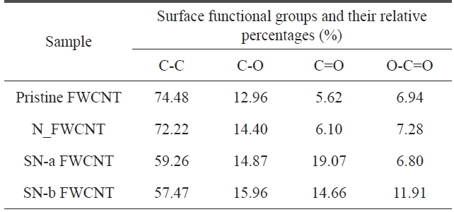
The C1s peak of pristine and acid-treated FWCNTs at 285 eV can be deconvoluted into four fitting curves with binding energy at ~285 eV, ~285.63 eV, ~286.59 eV, and ~289.16 eV, which are assigned to C-C, C-O, C=O and O-C=O, respectively (Fig.2 ) [19]. The relative amount of functional groups could be calculated from the area of each deconvoluted peak. The rela-tive amount of functional groups and the atomic element in the samples is listed in Tables 4 and 5, respectively.
As seen in Table 4, we found that the relative amounts of C-O and O-C=O on the surface of acid-treated FWCNTs are higher than that of pristine FWCNT. Furthermore, sulfuric/nitric acid-treated FWCNTs (indicated by SN-a FWCNT and SN-b FW-CNT) have much higher relative amounts of C-O and O-C=O than nitric acid-treated FWCNT (indicated by N_FWCNT). Moreover, the atomic percentage of the oxygen element (Table 5) on the surface of acid-treated FWCNTs noticeably increases compared to pristine FWCNT. These results indicate that acid treatment with sulfuric/nitric mixture acid could effectively in-
duce more polar oxygen-containing groups on the surface of nanotubes, which will improve the stability of CNT dispersion in DMF.
3.1.2. Carbon ordering
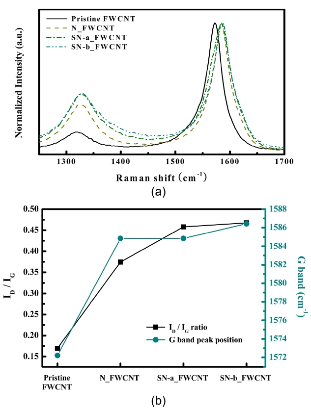
Raman spectroscopy is a powerful measurement method for evaluating the structural properties of CNT because it is a non-destructive and contactless measurement method. The CNT was formed through the crimping of flat graphite and has an unsatu-rated double-bond structure on the graphitic structure; thus a characteristic band can be measured using the Raman spectra. The peak near 1580 cm-1 represents the graphite E2g symmetry of the interlayer mode, which reflects the structural intensity of the
In this study, Raman spectroscopy was used to assess the qual-ity of FWCNTs depending on the acid treatments. Fig.3 a shows the Raman spectrum of pristine and acid-treated FWCNTs. The maximum Raman peak near 1570 cm-1 (
In addition, as shown in Fig.3 b, sulfuric/nitric acid-treated samples (SN-a FWCNT, SN-b FWCNT) have a higher ID/IG ratio than the nitric acid-treated sample (N_FWCNT), and the ID/IG ratio increases with increased refluxing time. These results in-dicate that the crystallinity of nanotubes could be triggered by a strong acid treatment and its experimental condition. In gen-eral, defects in nanotubes are mainly located at the tip due to the hemisphere structure of the carbon buckyball. Some defects can form on the side wall of the nanotube because of bending or kinking. These defects can be oxidized by a strong acid and then chemical functionalization can easily occur. Furthermore, these side wall defects can be an electron trapping site, which can be attributed to poor electron emission, even though the open tip of a nanotube has better emission properties than a closed one. In the Section 3.2, we will discuss the effects of nanotube crystal-linity on field emission properties.
3.1.3. Solubility and stability of FWCNT dispersion in DMF
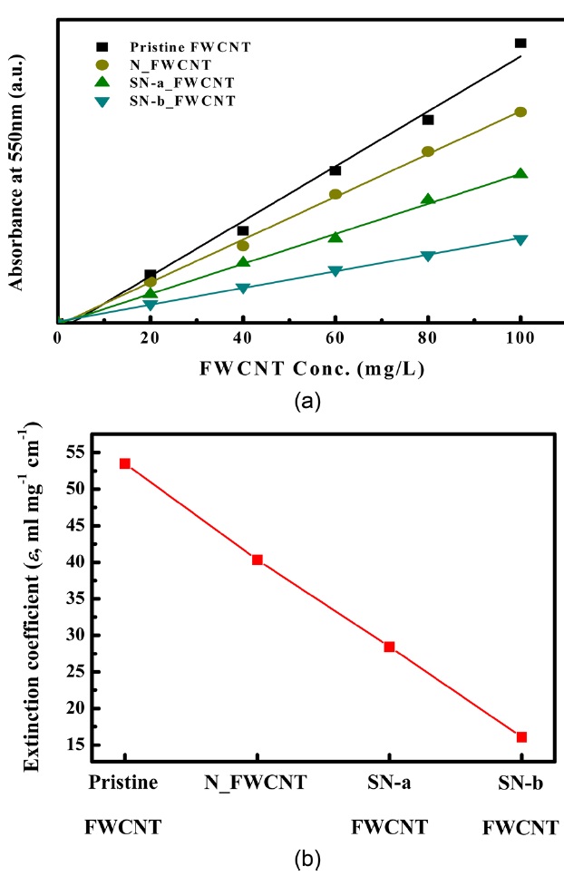
It is well known that the bundled structure of nano- tubes does not actively absorb light in the UV-Vis region; individual nano-tubes show the opposite effect [22]. Therefore, dispersion of CNTs can be characterized using UV-Vis absorption spectros-copy. In this study, to characterize the dispersion of FWCNTs in DMF using UV-Vis spectroscopy, absorbance values were re-corded at 550nm, as reported in previous studies [23, 24], which is shown in Fig. .4 According to the Beer-Lambert's law (
Fig.4a depicts the UV-Vis spectra of pristine and oxidized FWCNTs solution with various concentrations of nanotubes in DMF. We note that the relationship between the absorbance and the concentration of the FWCNT solutions was linear, which is in good agreement with Beer-Lambert's law [25]. In addition, it is noteworthy that the UV absorbance value of pristine FWCNT so-lution was higher than that of the oxidized FWCNTs solution;therefore, the extinction coefficient of the pristine FWCNT solution at a nanotube concentration of 100 mg/L is the largest (Fig.4b). We note that the absorbance of the nitric acid-treated sample (N_FWCNT) was higher than that of the sulfuric/nitric acid-treated samples (SN-a FWCNT, SN-b FWCNT) at the
same nanotube concentration (Fig.4 ). In general, carbon atoms in the pristine CNTs are in an
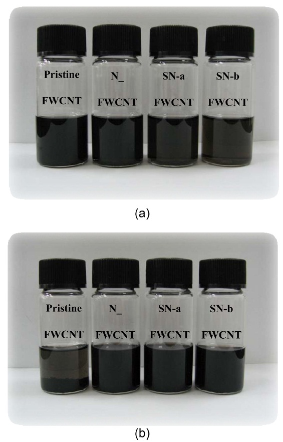
Fig. 5 shows the visual examination of pristine and oxidized FWCNTs in DMF at a nanotube concentration of 100 mg/L and 200 mg/L, respectively. Digital photo-images were taken after 24 h. It was found that the clear dispersion of pristine FWCNT in DMF was formed when the nanotube concentration was 100 mg/L, but in a higher concentration of 200 mg/L, the nanotubes were aggregated and precipitated. On the other hand, the oxi-dized FWCNTs showed a clear dispersion independent of the nanotube concentration in DMF. The stability of oxidized FW-CNTs in DMF may be due to the fact that the oxidation process introduces carboxyl and hydroxyl groups on the nanotube sur-
faces. These groups ionize in DMF and the oxygen-containing groups are negatively charged. The electrostatic repulsive forces between negative surface charges of the oxygen-containing groups may lead to the stability of oxidized nanotubes so that the oxidized nanotubes can form a stable dispersion in DMF. This suggests that the oxidized FWCNTs have high dispersion stabil-ity in DMF so that the aggregation could be minimized. Conse-quently, when the CNTs are oxidized by an acid treatment, the dispersion stability in DMF is significantly enhanced due to the combination of polar-polar affinity and electrostatic repulsion.
3.2. Characterization of FWCNTs/TEOS thin film field emitter
3.2.1. Morphological property
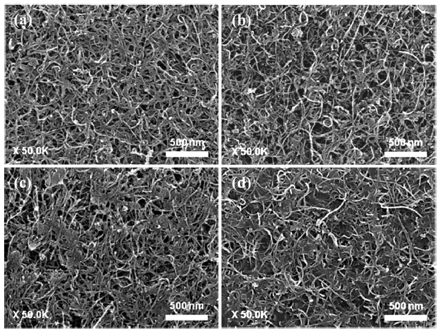
Fig. 6 shows the FE-SEM images of the spray coated FW-CNTs/TEOS films before the activation process. As increasing the oxidation level (or ID/IG), the TEOS binder was shown in the top of the film. The intermolecular interaction of TEOS with nanotubes is quite poor, so that the TEOS binder should be pre-cipitated to the bottom of the film. However, CNTs functional-ized with carboxyl or hydroxyl groups could interact with the TEOS layer precipitated to the bottom of the film, which is very low in the case of highly oxidized sample, as shown in the Figs.
6c and d. We also realized that the adhesion strength between CNTs and the substrate is varied depending on these oxidation levels. Therefore, following the activation process using the tap-ing should be optimized to minimize this adhesion effect on the field emission of CNTs.
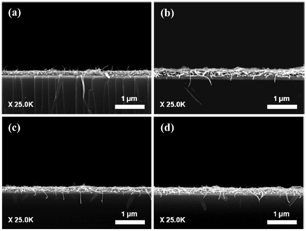
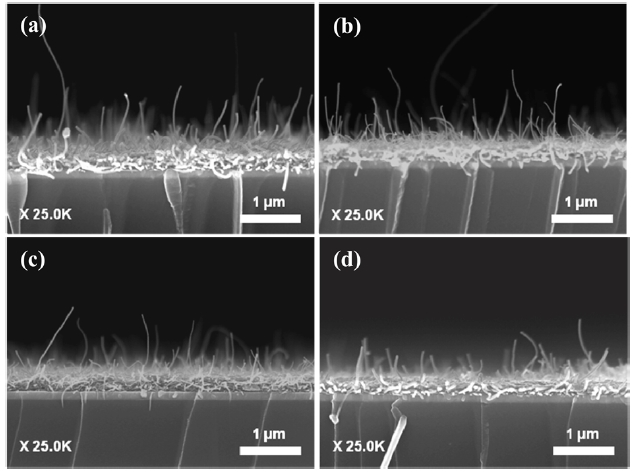
Figs. 7 and 8 show the cross-sectional FE-SEM image of the spray coated FWCNTs/TEOS-based field emitter before and after the activation process. The thickness of FWCNTs/TEOS film was about 0.3 μm. It was difficult to observe the protruded CNTs at the film surface before the activation process. The bur-ied nanotubes on the surface have been aligned by the removal of a covered layer, by applying the adhesive tape technique. As explained previously, this taping process was individually optimized to all samples. The surface morphology of activated FWCNTs/TEOS-based field emitter is shown in Fig. .8 After the
activation process, the film thickness slightly decreased from its original value of about 0.3 μm to about 0.2 μm, and many CNTs were preferentially aligned to the vertical direction. The aligned nanotube density of pristine FWCNT (Fig.8a), nitric acid-treated FWCNT (Fig.8b) and FWCNTs treated with sulfu-ric/nitric acid for a short time (Fig.8c) is quite similar, but the FWCNTs treated by sulfuric/nitric acid for a long time (Fig.8d) have low aligned nanotube density even though we sprayed the same amount of nanotube solution and optimized the activation process. The vertical alignment of the nanotube is necessary for its field emission application because high field enhancement is strongly related to the aspect ratio of the nanotube in the ver-tical direction. The emission stability of CNT emitters is also enhanced after the activation process because some loosely bounded nanotubes could be efficiently removed.
Therefore, the activation process of the CNT film is an important step in making a high performance nanotube field emitter.Vertically aligned CNT emitters are aged electrically inside a vacuum chamber to produce a uniform length distribution,which results in the stable emission of electrons even at a high electric field. During this electrical aging step, some protruded nanotube emitters, as shown in the Figs.8 a and b are oxidized through Joule heating.
3.2.2. Field emission properties of FWCNTs/TEOS thin film field emitter
Field emission results are usually analyzed by the
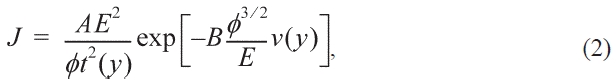
where
stants
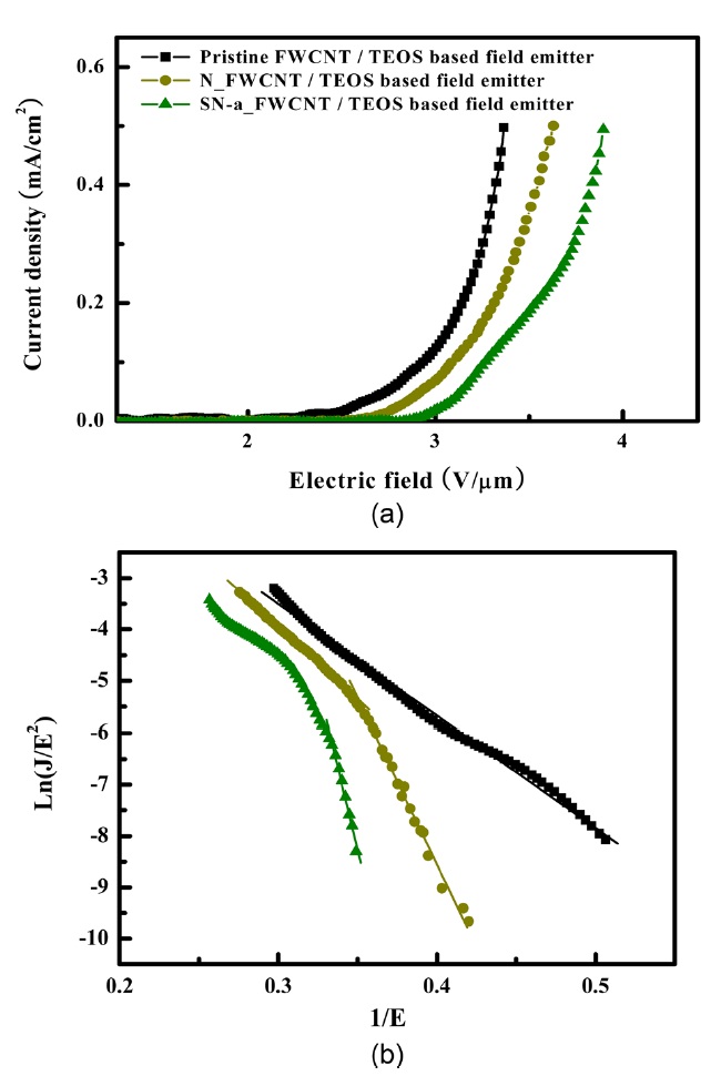
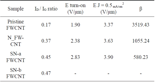
The field emission characteristics of pristine and oxidized FWCNTs were measured after electrical aging in each sample as shown in Fig. 9 and Table .6The vertically aligned pristine FWCNT/TEOS field emitter shows a low turn-on voltage of 1.90 V/μm, high field enhancement factor of 3519.43, and high emission current density of 0.5 mA/cm2 at an applied field of about 3.37 V/μm. On the other hand, the nitric acid-treated FW-CNT/TEOS (N_FWCNT) field emitter shows a turn-on voltage of 2.38 V/μm, field enhancement factor of 1055.24, and emis-sion current density of 0.5 mA/cm2 at an applied field of about 3.63 V/μm. A more excessively acid-treated FWCNT (SN-a FWCNT) compared to N_FWCNT shows the turn-on voltage of 2.83 V/μm, field enhancement factor of 580.23, and emission current density of 0.5 mA/cm2 at an applied field of about 3.9 V/μm. The field emission of FWCNT treated with sulfuric/nitric acid for a long time (SN-b FWCNT) was not observed due to the low aligned nanotube density and high defect ratio. The oxidized FWCNTs-based field emitter indicates higher turn-on voltage than the pristine FWCNT-based field emitter because
The ratio of the D-to-G band intensity and field emis-sion characteristics of the pristine FWCNT/TEOS and oxidized FW-CNTs/TEOS based field emitters
of the defects on the nanotube surface. There are two possible explanations. First, the defects located on the side wall of nano-tubes can act as an electron trapping site. It is well known that in an ideal nanotube, ballistic electron transfer is realized. That is why the electrical conductivity of nanotubes is extremely high. However, when the nanotube is treated with a strong acid, defects are formed in its side wall, and then the electrons are scattered and/or trapped. Finally, the conductivity of a defective nanotube is lower than that of an ideal one. In the field emission,the conductivity of emitters is also a very important physical property. Second, vertical alignment of nanotubes could be al-tered by a defect. The defects in the side wall of the nanotube mean that pentagons and heptagons are generated, and this re-sults in the bending of the nanotube with a certain angle to the vertical nanotube axis. In general, it is well known that vertically aligned nanotubes have much lower turn-on voltage and higher field enhancement factors than randomly entangled CNTs, indi-cating that most electrons are emitted from the tips of FWCNTs and the electronic DOS of tips near the Fermi energy is different from that of side walls [29]. Therefore, vertically aligned CNTs without defects can be used as highly effective field emitters.
The
several papers to explain this phenomenon [30, 31]. In our case, we can claim that this is related to desorption at a high elec-tric field. At a high electric field, the emission current increases, and thus Joule heating occurs especially at the nanotube tip. In general, intrinsic nanotube emission properties are revealed af-ter desorption of water molecules. However, water absorption is favorable to acid-treated nanotubes due to the polar-polar in-teraction between functional groups and water molecules. That is why pristine FWCNTs do not have a hetero-behavior of the field emission.
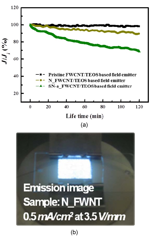
We have also compared the emission current stability of oxi-dized FWCNT-based field emitters with that of pristine FW-CNT-based field emitters with a constant field at 0.35 mA/cm2 of current density for 2 h. Fig.10a shows the degradation rate of the emission current density
We have discussed the influence of FWCNTs treated with ni-tric acid/sulfuric acid on field emission characteristics. Carboxyl and hydroxyl groups were functionalized on the surface of the FWCNTs using nitric acid and sulfuric acid in different propor-tions. When the FWCNTs are functionalized with carboxyl and hydroxyl groups, the dispersion stability in DMF was signifi-cantly enhanced due to the combination of polar-polar affinity and electrostatic repulsion.
In addition, FWCNTs/TEOS thin film field emitters were fab-ricated by a spray method using FWCNTs/TEOS one compo-nent solution onto ITO glass. After thermal curing, they were found tightly adhered to ITO glass, and after the activation pro-cess by a taping method, CNTs were aligned preferentially in the vertical direction. The FWCNTs/TEOS-based field emitter with uniform surface, small thickness and strong adhesion to the substrate was successfully fabricated using a spray method. The pristine FWCNT/TEOS-based field emitters revealed a higher current density, lower turn-on field, and higher field enhance-ment factor than the oxidized FWCNTs-based field emitters. However, the unstable dispersion of pristine FWCNTs in TEOS/DMF solution made them poorly applicable to field emitter fab-rication using the spray method. Although the field emitter of nitric acid-treated FWCNT showed slightly lower field emis-sion characteristics, this can be improved by introducing metal nanoparticles or a resistive layer coating.
Thus, we can conclude that our spray method could be use-ful for fabricating field emitters, which offer several advantages compared to previously reported techniques such as CVD and screen printing. For example, as well as a uniform surface, a convenient method to deposit CNTs for cathodes, and good re-producibility, it is cost-effective and amenable to mass produc-tion, and it could potentially lead to the use of CNTs as func-tional devices.