With countless numbers of scientific journals and patents spewing out each year, graphene has received undivided attention from the scientific and engineering applications communities, ever since the experimental confirmation of its existence. The discovery of the two dimensional, single atom layer-thick graphite with well-ordered honeycomb crystal lattice has shattered the previous arguments made by Peierls [1], Landau [2], Geim and Novoselov [3] that two-dimensional (2D) materials are thermodynamically unstable and cannot exist in a free state. Such a paradigm shift was already a tremendous attention gatherer. With the fortuitous discovery of single layer graphene, other 2D crystals were also discovered soon after [2,4,5]. Nevertheless, what made graphene the superstar of 2D crystalline materials are the unusual electrical and physical properties and the seemingly innumerable possibilities of new applications that may be brought forth by such properties. Some of the characteristics that excite scholars of graphene are its high intrinsic carrier mobility (200 000 cm2v-1s-1) [6,7], high thermal conductivity (~5000 Wm-1K-1) [8], high Young’s modulus (~1.0 TPa) [9], and high optical transmittance (~97.7%) [10], just to name a few.
The theoretical ground of graphene has been studied for 70 years [1,2] and it was already predicted that the charge carriers of two dimensional graphene sheet would behave like a massless Dirac fermion rather than follow the Schrodinger equation, which successfully directs most other materials’ quantum properties [3]. But up until Novoselov et al. [4,5] proved the existence of such a material, graphene was all but a theoretical model.
The first discovery, or the first synthesis method, of graphene came from a rather simple technique. This method, micromechanical exfoliation of highly oriented pyrolytic graphite (HOPG), involves repeatedly pulling apart graphite flakes into progressively thinner layers with Scotch tape until a few layers of graphene are obtained and placed onto silica wafers. The lateral size of such graphene can be up to 10 μm (Fig. 1) [4].
Although more complicated, another innovative micromechanical method involves running a modified atomic force microscope cantilever with HOPG graphite tip in contact mode on silica wafer to obtain 10-100 nm thick graphite crystallites [11]. Fig. 2 shows a scanning electron microscope (SEM) image of the modified cantilever and fabricated graphene.
Despite the relative simplicity of the techniques, graphene was not discovered earlier because not only is a single layer substance certainly not visible to the naked eye, but it is also nearly impossible to search for using small probes among mounds of other thick graphite pieces due to its small size [12]. The discovery of graphene, then, is in part due to another critical factor: the optical property of graphene, by which even a single layer is distinguishable in color under an optical microscope when put on a silica wafer of a certain thickness (300 nm) [3]. The graphene found in this way opened the door to the exploration of its properties and to empirical validation of its conceptual theories (theories such as graphene band structure of two cones meeting together at a Dirac point, where the effective mass of electrons reaches zero). Most notably, its half integer quantum Hall effect and the ‘relativistic’ nature of its charge carriers were experimentally recorded and studied extensively [11].
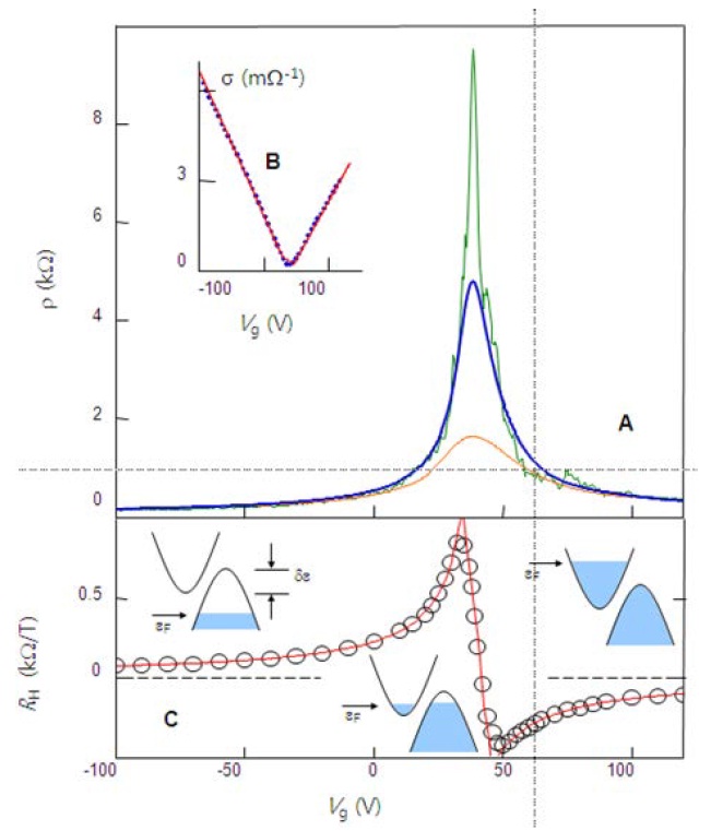
The study that resulted in the first device made by Novoselov et al. [4] from a few exfoliated layers of graphene was also fascinating. It showed ballistic transport phenomenon at submicrometer distances with a carrier mobility ranging from 3000 cm2v-1 s-1 to 10 000 cm2v-1 s-1. The device also manifested properties similar to that of the ambipolar field effect in semiconductors, showing a sudden sign change of the Hall coefficient at Vg, where the resistivity has a sharp peak and the conductivity
increases with the increasing gate voltage from both sides of the resistivity peak. Interestingly, the device did not show a zero-
conductance region but rather intrinsically exhibited an intermediate state at which the device was a mixture of holes and electron conductors (Fig. 3). As an attractive quality of a graphene device, its electronic characteristics can be tuned by applying a varying gate voltage, changing the device from purely electron or hole conductor to mixed hole-electron conductor.
As seen from the few discovered examples of compelling electronic properties of graphene, exfoliation from HOPG provides graphene with the quality and size that satisfy the needs of scientific research. With such needs met, many of the succeeding synthesis efforts were geared toward producing larger, uniform, and mass-producible graphene sheet in the hopes of meeting the commercial need for graphene in various applications in the future.
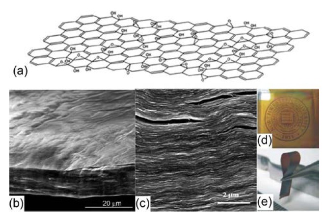
The idea of exfoliating a layer of graphene from graphite to obtain graphene quickly expanded to other variations such as chemical exfoliation [13]. This method utilizes strong acids and oxidants to produce graphene oxide (GO) from graphite. GOs have oxygen and hydroxyl groups attached to the interplanar surfaces of single graphitic layers (Fig. 4a). This makes graphene interlayers hydrophilic and allows easy intercalation by water molecules upon light sonication. Aqueous colloidal suspensions of single layer GO sheets (each is about 1 μ (in lateral dimension) are then produced. GOs made this way are non-conducting but can be reduced with organic reductants such as hydrazine. Unlike the micromechanical exfoliation method, the chemical method opened the possibility of producing graphene in relatively large quantities fairly quickly, not only for scientific purposes but for electronic applications as well. Reduced GOs can be dispersed onto desired substrate or filtered into free standing paper-like materials [14]. Such materials can be utilized as conductive thin films. An image of paper-like GO is shown in Fig. 4. Other methods use alkali ions [15,16] to intercalate or microwave [17-19]
the graphite to create puffed graphite layers in an effort to create a scalable production method of single layer graphene.
Despite the relative ease with which reduced GO can be made, the quality of the graphene sheets that are made is not so high. Because small suspended graphene particles are dispersed onto a substrate, the substrate does not have an orderly crystal structure or uniform thickness. Graphene provided by micromechanical exfoliation from HOPG still provides better quality graphene with a well-preserved crystalline structure. Thus the efforts to improve graphene synthesis continue.
As a more scalable approach was sought, and epitaxial growing of graphene by thermal decomposition of SiC received attention. Epitaxial growth of thin films on crystalline structures has been around for a long time [20-22]. Even before free standing graphene was obtained from the exfoliation method, surface science has driven the growth of single crystalline (but not truly monolayer or free standing), homogeneous growth of epitaxial graphite layers, as opposed to HOPG graphene, which has a polycrystalline structure resulting from in-plane azimuthal disorder [23-25]. As the optimization for epitaxial single layer graphene growth became feasible, several transfer methods appeared afterwards, making it possible to obtain free standing epitaxial graphene on desired substrates.
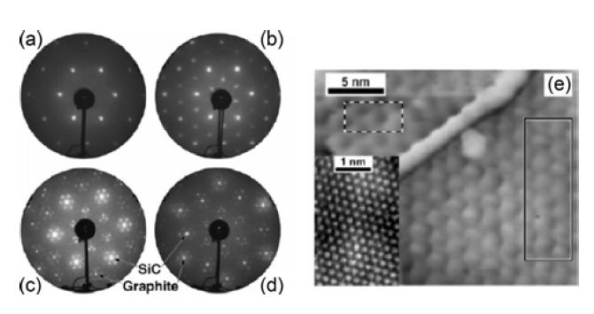
Analysis of experimental results from low-energy electron diffraction (LEED), grazing incidence X-ray diffraction, and scanning tunneling microscopy confirmed the highly ordered, single crystalline structure and relatively smooth and flat surface of epitaxially grown graphite on SiC (Fig. 5) [20-22,26]. The study opened the possibility of growing macroscopic sized growths of single graphene planes.
Work by Berger et al. [26] reported that several layer graphite grown under ultra-high vacuum (UHV) condition at temperatures of 1250-1450℃ on Si-terminated face of single-crystal 6H-SiC exhibited measured electron mobility of about 1100 cm2v-1 s-1, which is an acceptable value for some electronics applications.
Initially, Lee et al. [27] used a procedure similar to that em-
ployed for micromechanical exfoliation to transfer the epitaxially grown graphene on SiC onto silica substrate. But this method had the same limitation as the graphene produced with the exfoliation method: submicron size peeling of graphene layers limited the size of the transferable graphene.
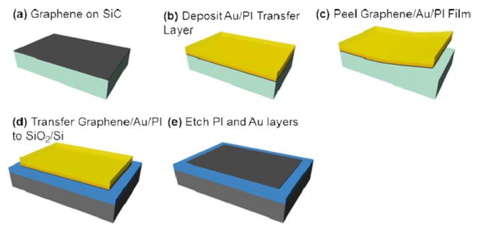
Another group [28] applied a thin gold layer and polyimide support onto epitaxial graphene to peel it off. The peeled Au, polyimide, and graphene layer were orthogonally etched (Fig. 6 for schematic diagram). But this process was also size limited due to the relatively weak adhesion of Au on the graphene surface. The transferred graphene also had high defects and a very low mobility of ~100 cm2 v-1 s-1. High defects may have resulted from the process of pulling graphene from the metal surface.
As an alternative transfer process [29], thermal release tape was used instead of conventional tapes. With this process, graphene on SiC was transferred with relatively few defects, as indicated by the low intensity of the Raman D-peak. Although the process was reliable because it removed almost all (leaving only a few layers behind on SiC) of the grown graphene from the SiC surface, it was not so desirable because obtaining thin single layer graphene was favored over many-layered graphene, which essentially is a kind of common graphite.
Recently, in order to overcome such a problem, a layer-by- layer transfer method was developed [30]. This enhancement was made possible by replacing Au, in the process mentioned above, with Pd. The new method provided better transfer results, reducing the graphene defects.
3.3. Chemical vapor deposition takes flight
Despite the betterment of the exfoliation and epitaxial growth on SiC, graphene samples grown with these methods were largely limited by total producible size. As a large-area producing method, chemical vapor deposition (CVD) growth first showed its potential in 2008 with CH4 as gaseous carbon source and Ni foil as the catalyst metal substrate. Although monolayer graphene growth had already been tried with various transition metals such as Co, Pt, Ir, and Ru [31-38], use of Ni is economically more viable and has better potential for upscale production. Although CVD growth of graphene on Ni started out “large” but was still 5×5 mm in size [39], with fervent research in its field, the producible size quickly grew to graphene with diagonal
width of 30 inches, and the use of Cu instead of Ni led to better controlled growth of mono or bi-layer graphene. Typically, the CVD method refers to thermal CVD (TCVD) but also, other CVDs that use plasma. Some of these include plasma enhanced CVD, radio frequency plasma enhanced CVD, inductive couple plasma CVD, surface wave plasma CVD [40], and microwave plasma CVD. In this paper, the focus is mainly on TCVD, which is the dominantly used method of CVD growth.
3.3.1. The metals
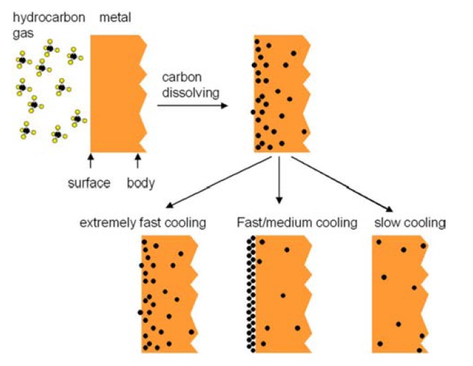
Currently the most widely used large scale method of CVD growth uses Cu or Ni. Because of the difference between Ni-C and Cu-C solubility, the two metals grow graphene with different mechanisms and produce graphene of different thickness and uniformity under the same conditions. Carbon atoms have relatively high solubility in Ni and consequently easily result in multilayer graphene growth rather than mono or bilayer. Ni films are typically brought to 1000℃ temperature in a hydrogen flow atmosphere (He or Ar is typically provided along with H2) and a carbon source is introduced for growth after the hydrogen annealing. Carbon atoms provided from the source gas reach the surface of the heated Ni substrate and diffuse into Ni, forming a carbon-nickel solid solution (Fig. 7). Because the solubility
of carbon in metal is a function of the temperature, lowering the temperature forces the absorbed carbons to precipitate on the metal surface. Here, the rate of cooling largely affects the quality and the number of graphene layers formed: the faster the cooling rates the greater the number of layers formed and the higher the defects. When the cooling rate is too slow (~0.1℃/s), carbon atoms are sequestered in Ni and are not given the chance to segregate on the surface, resulting in little or no growth [39]. On the other hand, in depth study [41] of the effects of cooling rates on graphene quality revealed that when the cooling rates are fast (25-100℃/s with 0.5-0.7 methane vol%), having many multi-layer islands form on graphene sheets while slowing down the cooling rate (<25℃) can reduce the multi-layer regions and produce relatively more uniform graphene sheets.
In order to produce controlled graphene layers using Ni, Kim et al. [42] presented the use of Ni film of various thicknesses (100-300 nm), which film was e-beam evaporated onto silica wafer; at the same time, they varied the growth time (time of metal exposure to carbon source). When the Ni layer was thick, more carbon was absorbed by the layer and thicker layers of graphene were formed. Therefore, with thinner Ni film and shorter growth time, monolayer graphene was grown, and with thicker Ni film and longer growth time, fewer layer graphene was grown. Thus the quantity of carbon absorbed into Ni was able to be limited by controlling the thickness of the Ni layer and the growth time.
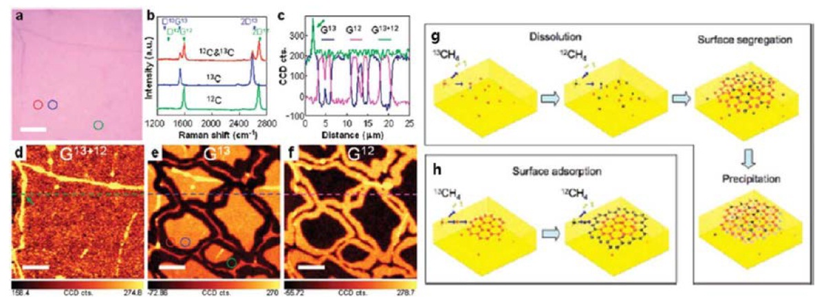
Li et al. [43-45] studied this mechanism in an intriguing way. Two different carbon isotopes, 12C and 13C, were introduced sequentially to the Cu and Ni substrates heated to around 1000℃ for growth. Raman intensity mapping was used to analyze the graphene surface to understand the growth mechanism. On Ni, graphene showed a random mix of 12C and 13C in its crystalline structure, implying that the carbon atoms were first absorbed into the Ni and randomly mixed before they were surface segregated. On Cu, graphene had rings of 12C and 13 Cregions, reflecting the same sequence in which the carbon sources were introduced (Figs. 8e and f). Such a result supported the hypothesis that graphene grows on Cu by surface adsorption and grows progressively outwards from the initial nucleation site (Figs. 8g and h shows the schematics of the different growth mechanisms on Cu and Ni). More interestingly, graphene growth seemed to be self-limited on a Cu surface when grown under vacuum conditions, effectively producing uniform single layer graphene with very few bi- or tri-layer islands. Later researchers found that such an effect does not necessarily apply to ambient pressure growth [46].
Much of the scientific community desires growth of monolayer graphene in order to study the unique electronic properties that strictly 2D graphene has. Graphene grown on Ni has a rather unsatisfying quality for such needs. Even with dominantly single- layer growth, the uniformity is low (many multi-layer patches are present) and this creates more intense Raman D-peaks. In this case, the use of Cu is better suited because it produces largely monolayer (around 90% coverage), uniform graphene with low D-peak intensity. On the other hand, when growing graphene samples for electronic applications such as touch screens, multilayer graphene is often desired. In this case, multi-stacking of Cu-grown monolayer graphene is useful because the increased number of graphene layers stacked in this way increases the electron mobility, although at a cost of reduced transmittance [47]. Growing multi-layer graphene on Ni is possible but once again produces low quality, relatively less uniform graphene with reduced electron mobility and high resistance.
3.3.2. Transferring
Perhaps the total producible size of graphene may not have increased so quickly if proper transfer methods had not developed together with the improvements of CVD methods. In the early stages, grown graphene samples were small and simple coating of polymer effectively supported the thin layers for transfer. For example, Yu et al. [39] deposited polymerized siloxane to support graphene and etched the Ni metal in HNO3 solution in order to transfer graphene onto a glass substrate. Another group
spin coated poly(methyl methacrylate) (PMMA) onto graphene and etched the Ni in HCl solution and then removed the PMMA coating in acetone. But this study reported relatively high defect density in graphene, resulting in high sheet resistance values (700-1000 Ω/sq). Such defects may have been caused by cracks generated during the transfer process or may have been due to the harshness of the etchant. The possible presence of nano ripples in graphene can also result in high intensity of the D-peak in the Raman spectra [44] (the D-peak is indicative of defects in graphene [48-51]), but the exact reason for the high defect density is unknown.
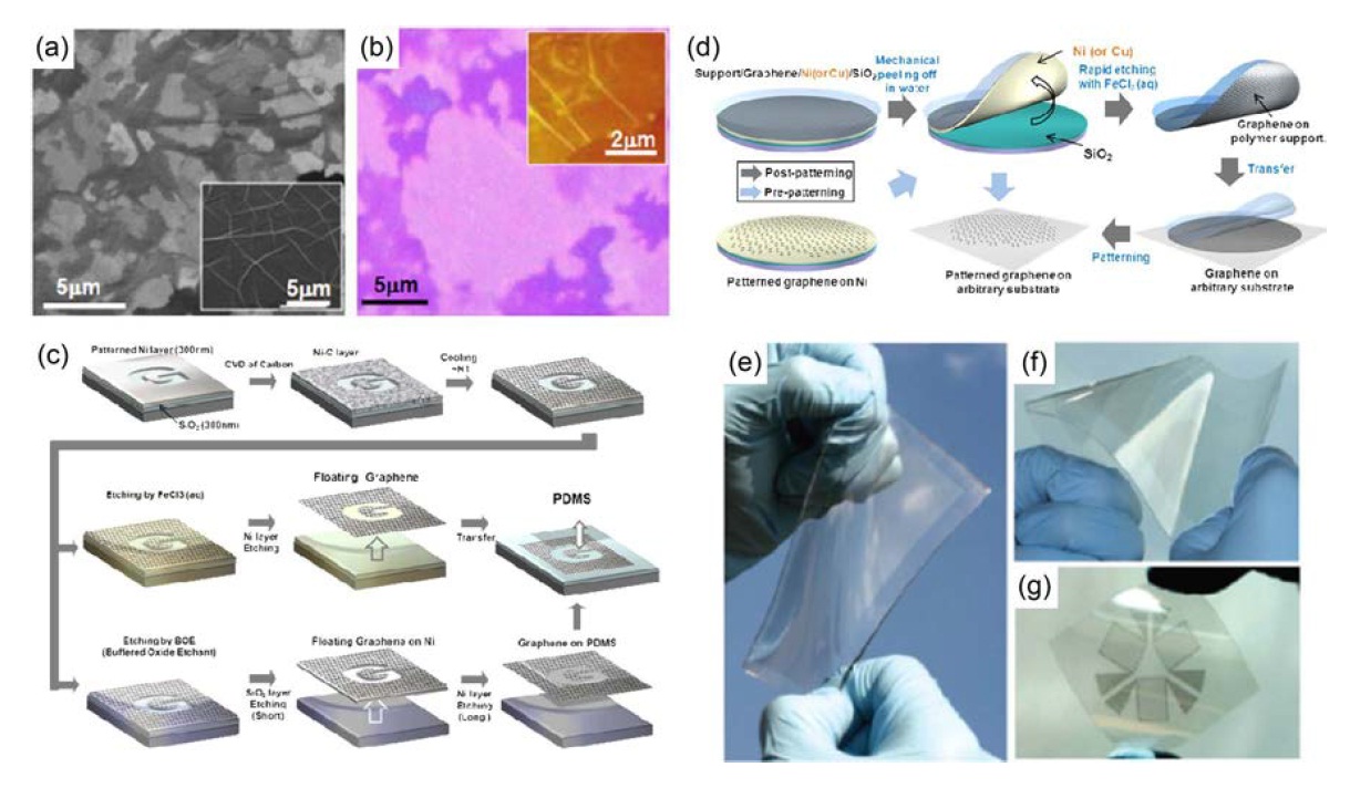
The defects from the transfer process were subdued when the polydimethylsiloxane (PDMS) stamping method was used (Figs. 9a-c) [42]. The sheet resistance measured was as low as ~280 Ω/sq and the Raman spectra showed almost no D-peak. After PDMS is applied to the graphene grown on Ni/SiO2 substrate, the metal layer is etched in FeCl3. The remaining graphene on PDMS separates and is ready for transfer onto desired substrates such as poly(ethylene terephthalate) (PET) or wafer. A Hall bar device made from graphene showed carrier mobility of ~3750 cm2v-1s-1 and the first observation of the CVD graphene half integer quantum Hall effect was performed. At the same time, graphene transferred onto a PDMS coated PET substrate showed excellent bending and strain resistance, showing stability of up to 18% tensile strain and 11% stretching strain. Along with the PDMS stamping method, dry transfer was also presented. It simply required etching of SiO2 and Ni in HF/BOE without the use of PDMS. Freed graphene can be easily scooped up on the desired substrate. In the later report, the use of gentle ultrasonication along with the PDMS stamping method significantly shortened the etching time and became the preferred method [52]. PDMS support and shortened etching time also became a reliable transfer method for the first wafer size graphene grown on Cu and Ni e-beam evaporated on SiO2/Si wafer (Figs. 9e and f).
Li et al. [47] multi-transferred and stacked up to four layers of graphene. While a single sheet of graphene had a sheet resistance of 2.1 kΩ/sq (measured using the van der Pauw method), multi-stacked four layer graphene had a low sheet resistance of 350 Ω/sq and still maintained 90% transmittance (more explanation of why the sheet resistance decreases with multiple stacking is given in detail in [47]).
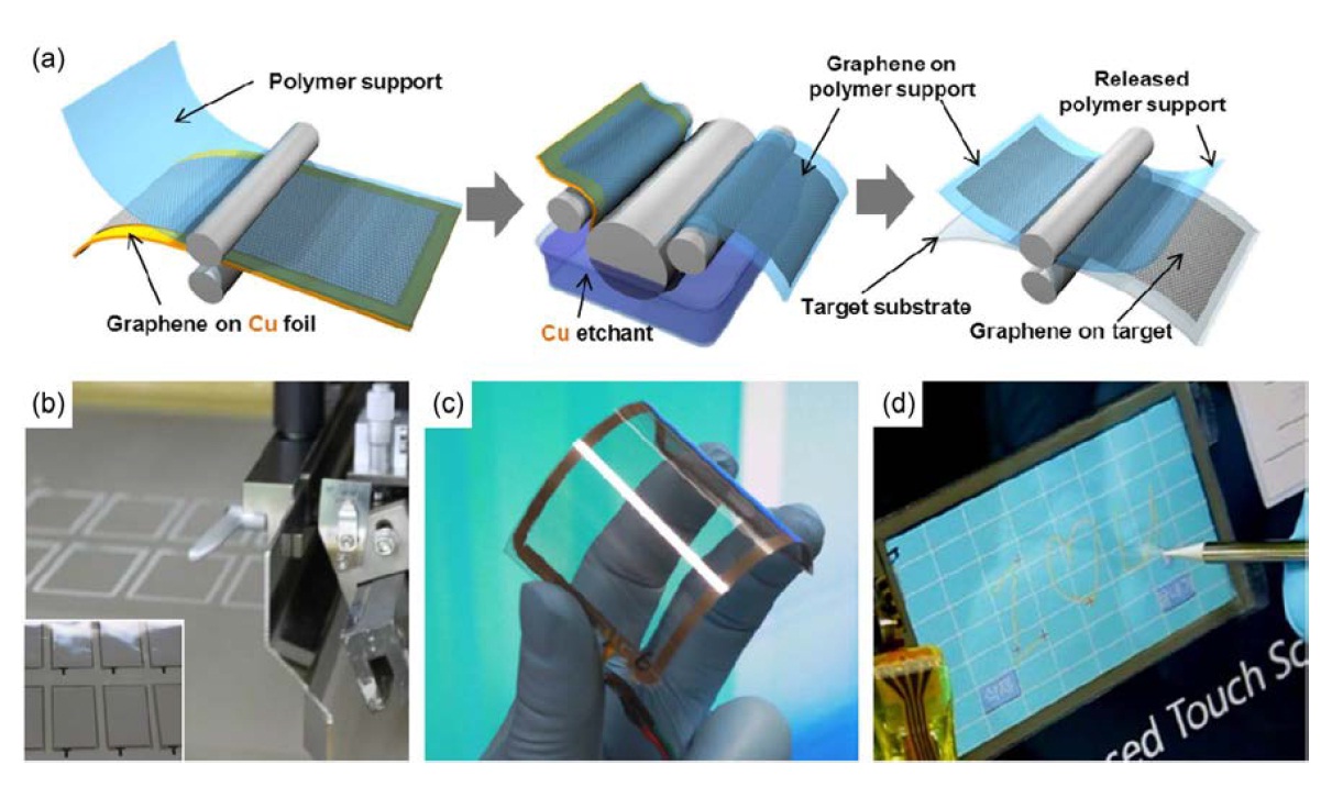
Because of the weak mechanical strength of spin coated PMMA, when the CVD growth with Cu foil succeeded in producing 30’’ large area graphene, it could not support the graphene of that size. PDMS stamping of large graphene was also not a suitable candidate method for transfer. Thus a new transfer
media was employed for ultra large scale graphene, thermal release tape [53]. The thermal release tape is sticky in its initial state and loses its adhesiveness upon gentle heating. The transfer steps are simple. Graphene on Ni or Cu foil is pressed onto the thermal release tape. After the metal is etched away, graphene on the tape is heat-pressed between rollers with the desired substrate (Fig. 10a). Graphene is left on the target substrate and the tape is released clean. Multi-layer stacking of graphene was also possible in this way. Raman study showed that the first layer transferred onto the PET substrate exhibits low conductance but subsequent layer stacking resulted in much improved conductance when compared to the multilayer stacked graphene transferred by PMMA coating. This implied that the first graphene layer interaction with the target substrate is not strong enough and therefore caused mechanical damage to the graphene when the thermal release tape was peeled away. However, subsequent layers do not interact directly with the substrate surface and transferred well onto the previous layer.
As-grown ultra large graphene boasts its best measured sheet resistance value of ~30 Ω/sq at 90% transmittance. Along with the half integer Hall effect of the graphene, the Hong group presented information on a promising potential for touch screen applications (Figs. 10c and d). The touch screen demo proved not only the excellent electronic quality of graphene, but also its unusual mechanical resilience.
3.3.3. Control and fine tuning
With the potential of full scale industrial size production of graphene on the horizon, recent efforts on CVD growth have been geared toward fine tuning the growth conditions, decreasing the defects, and understanding the science behind the growth mechanism.
In a sense, the desire to understand the growth mechanism of graphene itself is in part fueled by the aspiration to produce large graphene sheets with few defects. The theoretical study of the thermodynamics of graphene growth [54] predicts that the existence of any of the hydrocarbon species provided by methane (CH4, CH3, CH 2, and CH are referred to as CHx from this point on) is unfavorable on the Cu surface. It was calculated that rather than existing as an individual CHx species on Cu, the hydrocarbon species are thermodynamically more stable and stay in clusters of CHx. The minimum size of this cluster of CHx that results in a lower energy level is the critical nucleation size of carbons for graphene formation. Starting from the nucleation sites, graphene islands (typically called domain or grain) grow in size until the islands meet and eventually cover the entire catalytic metal surface. Currently, the exact mechanism of how the switch from CHx clusters to graphene occurs is not understood. Nevertheless, the findings opened the possibility of controlling the nucleation sites and numbers.
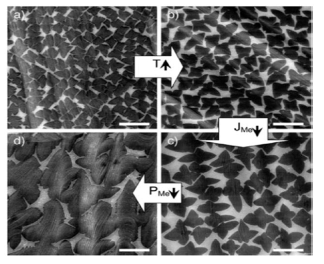
In a recent study [44], experiments were carried out to find growth conditions that can decrease the number of nucleation sites. The results revealed that under high temperature and low pressure and methane flow conditions, fewer nucleation sites were formed compared to conditions of higher pressure and methane flow. The experiment also involved increasing the size of each graphene domain. This is of interest because when two different domain boundaries meet upon full growth, they create defects on graphene (resulting in high D-peak in the Raman spectra), which is believed to be responsible for the high sheet resistance and electron scattering. Under higher pressure (still less than ambient pressure) and high methane flow, each domain
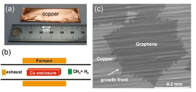
grew large fairly quickly. Thus, graphene was first grown under high temperature and low pressure and methane flow conditions in order to subdue the nucleation site formation ; the graphene was subsequently grown at higher pressure and methane flow conditions in order to enlarge the formed nucleation sites. This successfully resulted in full growth (meaning full coverage of the Cu surface) of graphene sheets with large domain size. The SEM images of the changes in domain density and size are shown in Fig. 11. From the reported SEM images, it can be seen that the domain size increased from ~5 μr to ~20 to with the growth condition adjustment. In their later report, Li et al. [55] grew a single crystalline graphene domain with dimensions of up to 0.5 mm on one side. The graphene was grown on the inside of the surface of a folded copper foil enclosure (Fig. 12). In this way, the growth was carried out under much lower methane pressure and “improved” conditions, in which the growth process is exposed to fewer impurities that may exist and also to higher concentration Cu vapor at static equilibrium. Raman spectroscopy confirmed the uniform monolayer growth and field-effect transistor measurements showed a high electron mobility of 4000 cm2 v-1 s-1
Another study that controlled graphene growth conditions [46] explored the effects of different pressure conditions on the layers of graphene formed on the Cu surface. The major finding of the study was that under ambient pressure, the growth resulted in thick graphene layers and a non-uniform surface, especially at high methane flow rate (lowering the flow rate somewhat increased the surface uniformity and decreased the layer thickness). Under low pressure and UHV conditions, typical growth was reproduced, creating nicely uniform, single-layer graphene. Thus, the previously reported self-limiting characteristic of graphene growth on Cu was found to be restricted to low pressure growth conditions.
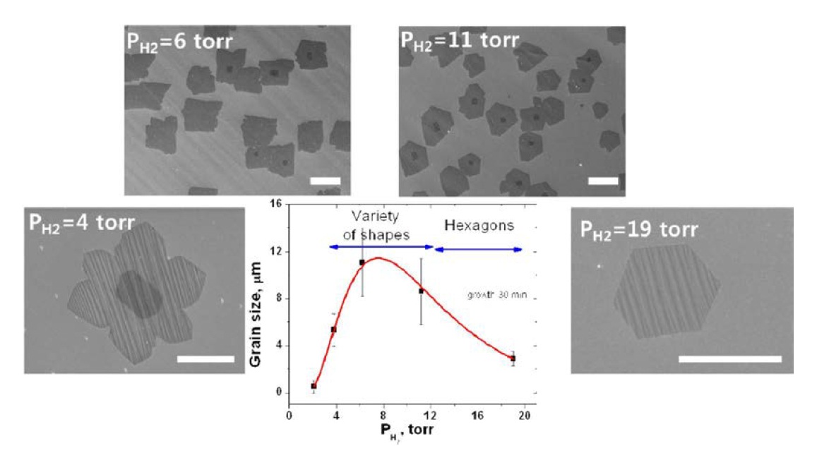
Lastly, one of the most recent notable findings is the identification of the role of hydrogen gas flow in CVD growth. Previous journals presenting their CVD growth methods mention the use of hydrogen gas flow for the purpose of annealing the metal surface. Work by Vlassiouk et al. [56] revealed the surprisingly critical roles that hydrogen play in CVD growth. First, hydrogen appears to be a co-catalyst of the metal in producing graphene. Under low hydrogen pressure (just enough to effectively anneal the metal surface), it was found that no graphene growth occurred when the methane pressure was very low (~30 ppm or 23 mTorr), although using high methane flow can drive the growth. Even at low methane pressure, however, when hydrogen pressure was larger than 2 Torr, graphene growth was detected. Second, hydrogen gas also acts as an etching reagent and controls the size and shape of graphene domains. Studies show that under moderate hydrogen pressure (PH2 of 4 and 6 Torr) domain shapes are highly irregular, and under high hydrogen pressure (PH2 of 19 Torr) domain shapes exhibit perfect hexagons (Fig. 13). The graphene domain sizes also reached a maximum under high hydrogen pressure and showed a uniform zigzag edge characteristic (under moderate hydrogen pressure, edges were mixed zigzags and armchairs). Thus the study reestablished hydrogen as an experimental control knob to produce graphene of desired crystalline shape and edges.
Yu et al. [57] took this further and produced uniform hexagonal shaped graphene domains using the nucleation seeded growth method. Raman analysis revealed that the boundary lines of zigzag edges of hexagonal graphene domains show smaller D-peak than do armchair edges, implying that the graphene with zigzag edges resulted in reduced defects and therefore exhibited better electronic qualities. Yu et al. [57] demonstrated a multiple electrode device made from two single crystal graphene domains sharing a boundary (Fig. 14). It was shown that because of the inter- domain boundary, the electron mobility is decreased and degrades the device performance. The group believes that improving the fabrication processes to make single crystalline, boundary-less, defect-subdued graphene sheet may be possible with further study.
Other than the aforementioned studies, persistent studies on topics such as the non-epitaxial nature of graphene growth, graphenesubstrate interaction, graphene doping, and work-function control are being reported. All of these studies will shed more light on how to control graphene synthesis and properties and help develop graphene as a truly usable material for future electronics.
3.3.4. Recent CVD techniques
Demonstration of a 30’’ scale graphene sheet has directed much focus to CVD growth on Cu using methane. But the on- going graphene synthesis research is not limited to this particular process alone. One of the methods receiving attention is the growth of graphene at low temperatures, as such a process would be less energy intensive and therefore favorable for industrial production. Graphene growth with solid and liquid carbon source has also been shown in recent studies and the use of these sources allows for good quality monolayer graphene growth at lower temperatures [58]. For example, PMMA was used as a solid source and monolayer graphene was successfully grown
at 800℃. Even at temperature ranges of 400-700℃, graphene growth was possible, although at some cost of reduced quality. The same study also successfully demonstrated growth using liquid benzene at temperatures below 800℃. Various plasma based CVD growth methods of graphene are receiving attention because of potential low temperature conditions, while maintaining high electron energy (also called electron temperature). As an example, the surface wave plasma CVD method was used to successfully synthesize large area (23 cm×20 cm) graphene at 300-400℃ [40]. Such studies pave the way to well-controlled, low temperature, low energy intensive graphene growth with flexible carbon source selection.
The search for new metal catalyst is also on-going and likely to continue expanding. Other than Ni and Cu, use of other metal catalyst such as Fe [59,60] and Co [61,62] is emerging (Fig. 15). One study showed controlled graphene layer growth using Ni-Cu alloy as metal substrate [63]. According to the study, at Ni composition of 5.5%, monolayer graphene was formed, at 10.4%, bilayer was formed, and at 18.9% multilayer graphene was formed. With further research precise control of graphene sheet as well as grain size may be achievable by employment of new catalysts.
Even with some loose ends and numerous aspects of research that need to be addressed, graphene still shows tremendous potential for applications in incredibly diverse fields.
The most soon-to-be realized application is the use of graphene as a conductive electrode. Excellent carrier mobility and electron conductivity mean that graphene will find many places in the electronics market. Currently, the touch screen and electrode fields are dominated by the use of indium tin oxide (ITO). When compared to graphene, ITO is easy to handle and tends to outperform graphene in terms of conductance and low sheet resistance at the current stage. However, graphene quality is expected to improve with the fine tuning of its synthesis process and its electrical properties are still at an acceptable level for several applications. Given this, graphene’s mechanical resilience, flexibility, and high transparency play important roles in establishing graphene as the new revolutionary material to replace ITO.
4.1.1. Touch screen
Demonstration of a graphene based touch screen first done by Bae et al. [53], which renders a graphene based electronics market something quite realistic. A palm-sized touch screen was made with a CVD grown graphene sheet. Even when the graphene sheet was predominantly single layer (this corresponds to the achievement of ~97% transmittance), it showed remarkable resilience upon bending and when written on with a touch screen pen. Bolstered by the roll-to-roll production possibility of graphene sheets on a large scale and given the reliable performance of the graphene touch screen, such industrial advancements seem very much feasible.
4.1.2. Light-emitting display/organic light-emitting display and solar cells
As a transparent, highly conductive material, graphene has its niche in the light-emitting display (LED)/organic LED (OLED) and solar cell research fields as well. Primarily, graphene is used as an anode electrode in experimental OLED applications in an effort to replace ITO, which is brittle and relatively unstable at ambient conditions. Graphene not only fulfills its function as an anode but also allows an OLED to be entirely transparent and flexible, expanding the design and application horizon of OLED lighting. Typically, solution suspended reduced GO is spin coated onto a ridged substrate such as glass or is mixed with conducting polymer and spin coated onto flexible PET [64,65]. Most of the current research shows that although the performance (light emitting efficiency, sheet resistance, electron leakage) is acceptable, graphene is still inferior when compared to ITO due to the roughness of the graphene sheet made from reduced graphene oxide (GO) and the uneven distribution of hole density [64-66]. These shortcomings are expected to be overcome with improvements of graphene synthesis and doping techniques, which would result in production of uniform high quality graphene with minimum roughness, with less resistance and controlled, uniform hole distribution.
Graphene can also replace ITO as a transparent current spreading layer in LED [67]. The outcome of such a replacement is improved transparency in the blue and near-infrared light regions and increased stability in acid and bases, as ITO tends to have these limitations. The graphene in this application model was synthesized by large scale CVD; it allowed easy patterning of graphene layers and batch fabrication of LED devices, taking
us a step near to mass production of LED.
The role of graphene is similar in solar cell applications. It functions as an alternate anode material that eliminates the limitations of the existing material. For example, graphene can replace ITO in organic solar cells or fluorine tin oxide in dye-sensitized solar cells [68,69]. Graphene provides high transparency, a smoother contact surface and high thermal stability. Or, graphene itself can be p-doped or n-doped to serve as a solar cell main component in which the photoelectronic reactions occur [70].
Graphene films have also been implemented to make flexible organic solar cells working as anodes. The resultant devices have achieved competitive performance compared with their counterparts that use ITO electrodes [71]. It has been revealed the graphene based organic photovoltaic devices can survive at a harsh bending condition of up to 138o and maintain their performance. On the contrary, devices with ITO-anodes were eliminated just at the bending condition at 36℃ (Figs. 16c and d). Researchers have found that the conductivity of graphene on flexible substrates has outstanding stability even after hundreds of bending cycles [72].
4.2. Flexible and stretchable electronics
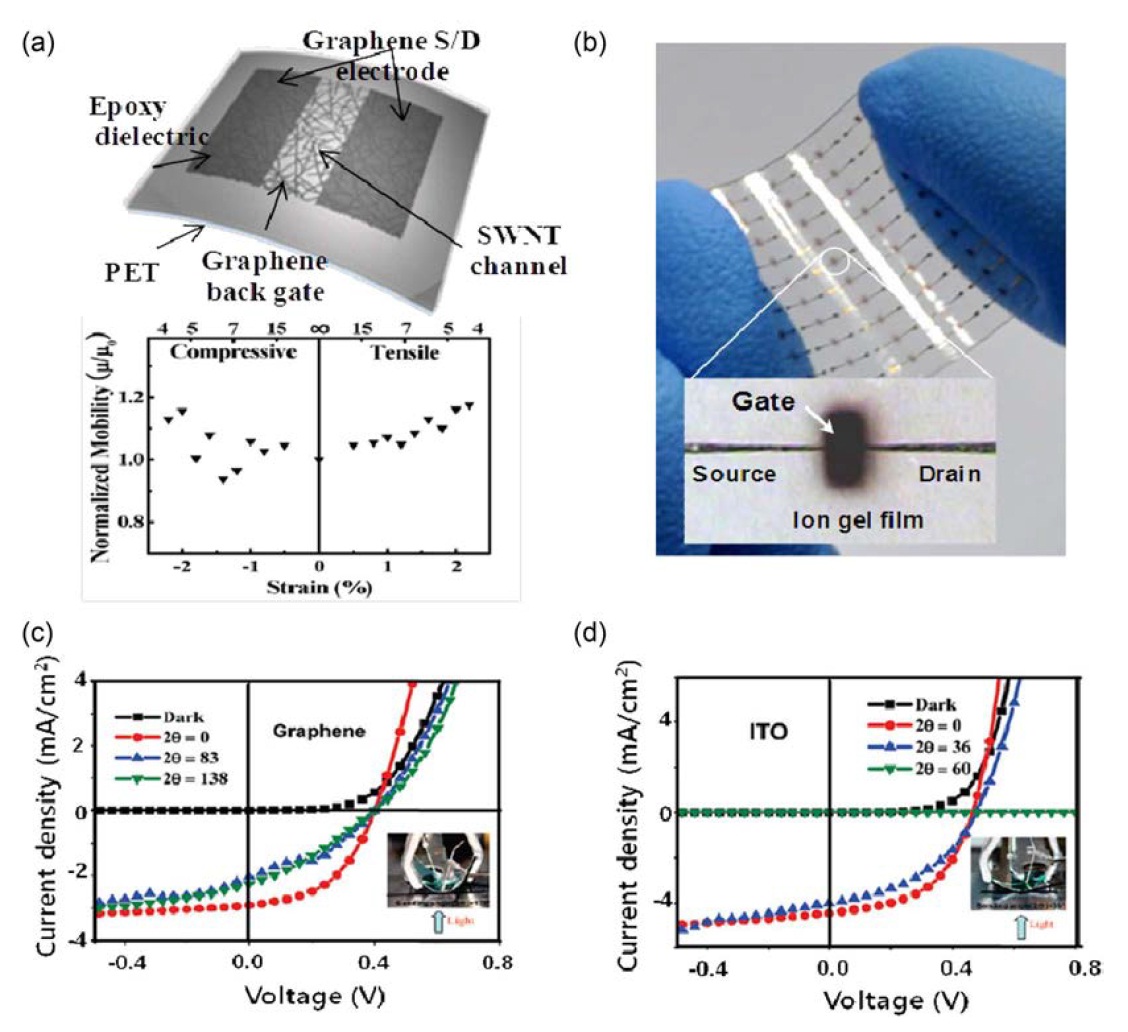
The properties of graphene allow great applications in the next generation of optoelectronics, in which flexibility and stretchability are essential. As mentioned above, CVD-grown graphene is a good candidate to replace ITO in transparent conductive electrode applications. The great advantage of graphene- based electronics is further demonstrated in flexible devices. An array of flexible field-effect transistors can be fabricated on PET substrates with graphene as source/drain electrodes and carbon nanotubes as semiconducting channel, as shown in Fig. 16a [73]. Such devices present high optical transmittance and mechanical bendability. The low contact resistance between graphene and organic materials makes graphene an ideal electrode material, especially in flexible organic field-effect transistors [74-78]. Another kind of graphene-based flexible transistor utilizes graphene as an active channel (Fig. 16b) [79]. A CVD grown graphene film was transferred onto pre-patterned Au source/drain electrodes and was isolated to make a channel region. Subsequently, ion-gel was spread as a dielectric layer and this process
was followed by gate electrode deposition.
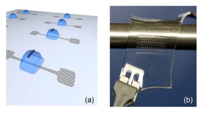
More recently, stretchable graphene-based devices have been developed [80]. The stretchable transistor was fabricated on PDMS rubber substrate with stretchable ion-gel as gate dielectric and graphene working as semiconducting channel as well as source/drain electrodes (Fig. 17). The devices presented excellent optical transmittance and stretchability that maintained the hole and electron mobility at 1100 and 360 cm2v-1 s-1, respectively, even at a strain level of ~5%. Graphene is also a good candidate for stretchable interconnects due to its intrinsically stable electrical property at high strain. Stretchable graphene interconnects have been successfully used in stretchable inorganic LED [81]. The stable operation of devices within the range of tested strain and repeated cycles indicated the robust stretchability of the devices without any structural deterioration.
Graphene also competes with its carbon relatives to make better supercapacitors. It is important that the material acting as electrochemical double layer used in the capacitor provide high specific surface area and high conductivity. Previously used activated carbon materials had high surface area but low conductivity. Carbon nanotube based supercapacitors also showed limitations of high contact resistance between carbon nanotube and the current collector. Using chemically reduced GO in hydrazine, on the other hand, provided high conductivity, large specific surface area and chemical stability, resulting in specific capacitance of up to 205 F/g in aqueous electrolyte [82]. Other supercapacitors were fabricated from chemically modified graphene with high surface area and achieved specific capacitances of 135 F/g [83] and 247 F/g [84] in aqueous electrolytes.
Owing to the cornucopia of fascinating properties that it has beyond merely its electrical ones, graphene shows an interesting variety of applications in the field of sensors and actuators. Just to take a few examples, graphene’s negative thermal expansion coefficient makes possible the fabrication of a microactuator that can be used to imitate biological movements. Zhu et al. [85] attached a patterned CVD grown graphene sheet to epoxy (with positive thermal coefficient), making a micro cantilever. When heat was provided from an electrical current, the difference in thermal expansion made the cantilever bend up and back down. This was further elaborated by the imitation of dragonfly wings made to move with the same concept. Another study [86] discovered graphene actuation induced by the strain from an electrostatic double layer under aqueous conditions. This demonstrated a possible use of monolayer graphene for nano electromechanical system actuators. Lastly, Wang et al. [87] fabricated highly sensitive strain sensors using graphene ripples. By applying graphene strips to a pre-strained PDMS substrate, they created evenly distributed graphene nano ripples. The sensor utilizes the fact that nano ripples (commonly viewed as defects in CVD grown graphene) increase the sheet resistance of the graphene due to the electron scattering that occurs at the ripples. Thus the strain sensing is done by monitoring the sheet resistance change with the changing strain that disturbs the nano ripple formations.
Graphene’s protective property has been noted since early on as it seemed to keep the Cu metal used in the CVD process from oxidizing or corroding [41,88,89]. This aspect of graphene has been further researched in depth and indeed has proved to yield an excellent oxidation resisting coating for metals such as Cu and Ni [90]. Furthermore, as discovered by Bunch et al. [91], graphene is impermeable not only to O2 but also to gas molecules as small as He. Not only high quality sheets but also crumpled graphene nanosheets have showed barrier potential when they were suspended in a polystyrene matrix [92]. The sheets effectively blocked the penetration of oxygen through the polymer-graphene mixture. The study shows a potential use of graphene as part of various gas barriers in the future.
One of the most unexpected uses of graphene is in biological applications. The recent findings of graphene’s ability to facilitate the differentiation of stem cells without interference of growth or alteration of the growth environment of the cells [93] have instigated more interest in graphene in the biomedical community. Not only that, the sensitive charge-carrier modulation of chemically modified graphene has allowed the development of bio-devices that can detect a single bacterium or that can sense DNA (for example, an attachment of a single bacterium on a fabricated biodevice results in the generation of 1400 conducting holes, which can be easily monitored) [94].
Fortuity may have led to the discovery of free standing graphene, but certainly the vigor and innovation in the research community have driven the rapid advances in graphene science and engineering since that first discovery. Although there remains a certain gap between graphene synthesized with current methods and knowledge and the graphene needed for practical applications, the progress of the research briefly overviewed in this paper assures continued improvements. Full implementation of graphene based electronics and consumer products may come about with the fine-tuning of the growth process, which will reduce damages that occur during etching and transfer and allow the acquisition of definite control over graphene’s electrical properties.

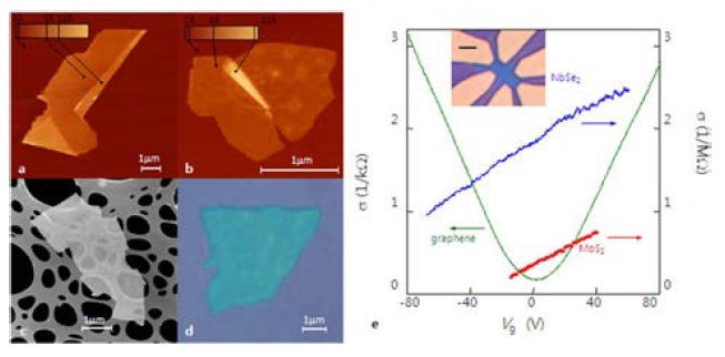
![Atomic force microscope images of various two-dimensional (2D) crystals discovered along with graphene. (a) NbSe2, (b) graphite, (c) MoS2, and (d) Bi2Sr2CaCu2Ox. The crystals are on 300 nm oxidized Si wafer except the MoS2, which is on holey carbon nulllm. (e) The graph shows the electric nulleld enullect in sheets of 2D crystals. The changes in electrical conductivity of NbSe2, MoS2, and graphene are shown as a function of gate voltage. It is clear that graphene has a distinct trend compared to other 2D crystals (inset is the device used to measure the conductivity) [5].](http://oak.go.kr/repository/journal/10989/HGTSB6_2012_v13n1_1_f001.jpg)
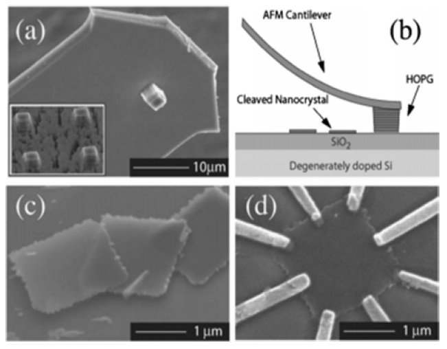
![Graphene micromechanical cleaving using atomic force microscope (AFM) tip. (a) Scanning electron microscope image of highly oriented pyrolytic graphite (HOPG) crystallite mounted on an AFM cantilever (inset is the bulk HOPG surface patterned by masked anisotropic oxygen plasma etching. (b) schematic drawing of the microleaving process using the modinulled AFM tip. (C) thin graphite nulllms obtained by the microcleaving process. (d) a mesoscoping device fabricated from the obtained graphite sample [6].](http://oak.go.kr/repository/journal/10989/HGTSB6_2012_v13n1_1_f002.jpg)
![Field enullect in a few layers of grapheme (FLG). (a) Relationship between FLG’s resistivity change and gate voltage for dinullerent temperatures at T = 5, 70, and 300 K, from top to bottom curves, respectively. (b) Example of changes in the nulllm’s conductivity obtained by inverting the 70 K curve. (c) Hall coenullcient as a function of gate voltage for the same FLG at T = 5 K [4].](http://oak.go.kr/repository/journal/10989/HGTSB6_2012_v13n1_1_f003.jpg)
![Graphene oxide (GO) sheets. (a) General chemical structure of GO; (b and c) low- and medium-resolution scanning electron microscope side-view images of ~10 micron thick GO sample; (d-f) digital camera image of GO paper; (d) ~1 nullm-thick (the Northwestern University logo is beneath the paper); (e) folded ~5 nullm-thick semitransparent nulllm [13].](http://oak.go.kr/repository/journal/10989/HGTSB6_2012_v13n1_1_f004.jpg)
![Thin graphite grown epitaxially on SiC. (a-d) Low-energy electron dinullraction (LEED) patterns from graphite/SiC(0001). Each represents sample that was heated several times to successively higher temperatures. (a) 1050℃ for 10 min; shows SiC 1×1 pattern at 177 eV; (b) 1100℃ for 3 min; shows √3 ×√3 reconstruction at 171 eV; (c) 1250℃ for 20 min; shows 6√3 × 6√3 pattern at 109 eV; (c) 1400℃ for 8 min; shows LEED pattern at 98 eV; (e) scanning tunneling microscopy image of a surface region of graphite grown on SiC [26].](http://oak.go.kr/repository/journal/10989/HGTSB6_2012_v13n1_1_f005.jpg)
![Schematic illustration of the steps for transferring graphene grown on an SiC wafer to another substrate by using the Au peeling method [28].](http://oak.go.kr/repository/journal/10989/HGTSB6_2012_v13n1_1_f006.jpg)
![Illustration of carbon segregation at metal surface such as Ni [39].](http://oak.go.kr/repository/journal/10989/HGTSB6_2012_v13n1_1_f007.jpg)
![Exploration of graphene growth mechanisms using dinullerent carbon isotopes. (a-f) Micro-Raman characterization of the isotope-labeled graphene grown on Cu foil and transferred onto an SiO2/Si wafer. (a) An optical micrograph of the identical region analyzed with micro-Raman spectroscopy; (b) Raman spectra from 12C-graphene (green), 13C-graphene (blue), and the junction of 12C- and 13C-graphene (red), respectively, marked with the corresponding colored circles in (a) and (e); (c) line scan of the dashed line in (d-f). integrated intensity Raman maps of (d) G13+12 (1500-1620 cm-1), (e) G13 (1500-1560 cm-1), (f ) G12 (1560-1620 cm-1) of the areas shown in (a). Scale bars are 5 nullm. (g-h) Schematic diagrams of the possible distribution of C isotopes in graphene nulllms based on dinullerent growth mechanisms for sequential input of C isotopes. (g) Graphene with randomly mixed carbon isotopes atoms such as might occur from surface segregation and precipitation (as expected for graphene growth on Ni); (h) graphene with carbon isotopes grown in the same sequence of input carbon source as might occur by surface adsorption (as expected for graphene growth on Cu) [43] .](http://oak.go.kr/repository/journal/10989/HGTSB6_2012_v13n1_1_f008.jpg)
![Chemical vapor deposition (CVD) graphene and wafer-scale synthesis and transfer. (a) Scanning electron microscope images of CVD grown graphene nulllms on thin (300-nm) nickel layers and thick (1-mm) Ni foils (inset). (b) An optical microscope image of the graphene nulllm transferred to a 300 nm thick silicon dioxide layer. The inset atomic force microscope image shows a typical rippled structure. (c) Synthesis, etching, and transfer process of the large-scale patterned graphene nulllms. Etching is done using FeCl3 and the transfer is done using polydimethylsiloxane (PDMS) stamp. Etching can be done using bunullered oxide etchant (BOE) or hydrogen nulluoride solution and dry-transfer of the graphene nulllms at room temperature. (d) Schematic illustration for fast etching and transfer of wafer-size graphene nulllms. Transferring and patterning of graphene nulllms grown on a metal/SiO2/Si wafer. Graphene/metal layers supported by polymer nulllms are mechanically separated from an SiO2/Si wafer. After fast etching of metal, the graphene nulllms can be transferred to arbitrary substrates and then patterned using conventional lithography. (e-g) Photographs of wafer-scale graphene nulllms. (e-f) The graphene nulllms printed on a poly(ethylene terephthalate) and a stretchable rubber substrate. (g) The three-element rosette strain gauge pattern on rubber by pre-patterning method [42,52].](http://oak.go.kr/repository/journal/10989/HGTSB6_2012_v13n1_1_f009.jpg)
![Roll to roll production of graphene and touch screen application. (a) Schematic of the roll-based production of graphene nulllms grown on a copper foil. The process includes adhesion of polymer support such as thermal release tape, copper etching (rinsing) and dry-transfer-printing on a target substrate. (b-d) Photographs of application of graphene nulllm grown by roll-to-roll method. (b) Screen printing process of silver paste electrodes on graphene/ poly(ethylene terephthalate) (PET) nulllms. The inset shows 3.1-inch graphene/PET panels patterned with silver electrodes before assembly. (c) An assembled graphene/PET touch panel showing outstanding nullexibility. (f) A graphene-based touch-screen panel connected to a computer with control software [53].](http://oak.go.kr/repository/journal/10989/HGTSB6_2012_v13n1_1_f010.jpg)
![Controlled growth of graphene domains. Scanning electron microscope images of partially grown graphene under dinullerent growth conditions: T (℃), JMe (sccm)/PMe (mTorr): (a) 985/35/460, (b) 1035/35/460, (c) 1035/7/460, (d) 1035/7/160. Scale bars are 10 nullm. As seen from the images, lower density of seed domain is achieved with higher temperature and lower methane nullow settings and large single crystal growth is achieved by lowering the methane partial pressure [44].](http://oak.go.kr/repository/journal/10989/HGTSB6_2012_v13n1_1_f011.jpg)
![Large single crystal growth of graphene. (a) Copper foil enclosure prior to insertion in the furnace for chemical vapor deposition (CVD) growth. (b) Schematics of the CVD system for graphene on copper. (c) Scanning electron microscope image of a large single crystal graphene on enclosed copper foil grown by CVD. The graphene domain is grown at 1035℃ on Cu at an average growth rate of ~6 nullm/min [55].](http://oak.go.kr/repository/journal/10989/HGTSB6_2012_v13n1_1_f012.jpg)
![Enullect of hydrogen on graphene grain (domain) shape. The average size of graphene grains grown for 30 min at 1000℃ on Cu foil using 30 ppm methane in Ar mixture at 1 atm, as a function of partial pressure of hydrogen. The nullgures illustrate scanning electron microscope images of the typical shapes under these dinullerent conditions. Note that perfect hexagons are observed only at higher hydrogen pressures. Irregularly shaped grains grown at low hydrogen pressure. Scale bars are 10 nullm (top two images) and 3 nullm (bottom two images) [56].](http://oak.go.kr/repository/journal/10989/HGTSB6_2012_v13n1_1_f013.jpg)

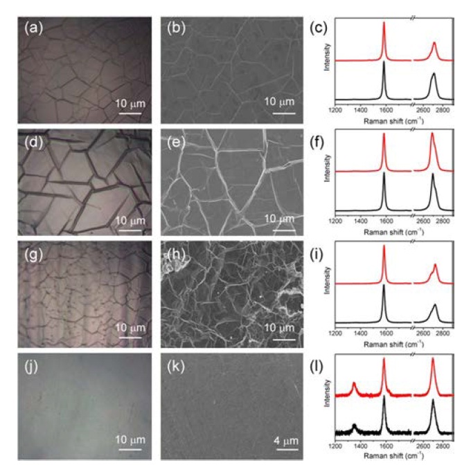
![Typical optical microscopy images, scanning electron microscope (SEM) images, and Raman spectroscopy of MLG and FLG grown on Ni (a-c), Fe (d-f), Co (g-i), and Cu (j-l) foil substrates using ethylene as the carbon source at 975℃. The growth time was 3 min, and the gas mixing ratio of C2H4/H2 was 5/500, and the cooling rate was 60℃/min. (a, d, g, and j) Optical microscope images of graphene. (b, e, h, and k) SEM images of graphene. (c, f, i, and l) Raman spectroscopy of graphene. Cu substrate background was subtracted. The spectra were normalized with the G- band [60].](http://oak.go.kr/repository/journal/10989/HGTSB6_2012_v13n1_1_f015.jpg)
![Graphene application for nullexible transparent nulleld-enullect transistor (FET). (a) Schematic structure of the nullexible FETs on the plastic substrate and the change in the normalized enullective device mobility null/null0 for TTFTs as a function of the bending induced strain and bending radius. (b) Optical images of an array of ion gel gated graphene FET devices on a plastic substrate. Current density vs. voltage characteristics of chemical vapor deposition graphene (c) or indium tin oxide (ITO) (d) photovoltaic cells under 100 mW/cm2 AM1.5G spectral illumination for dinullerent bending angles. Insets in c and d show the experimental setup employed in the experiments [71].](http://oak.go.kr/repository/journal/10989/HGTSB6_2012_v13n1_1_f016.jpg)
![Graphene for stretchable transparent transistor. (a) Schematic illustration of monolithically patterned graphene transistor. Ion gel is printed on channel region by aerosol printing method. (b) Photograph of stretchable ion gel gate dielectric graphene transistor array on PDMS substrate [80].](http://oak.go.kr/repository/journal/10989/HGTSB6_2012_v13n1_1_f017.jpg)