Graphene is an atomically thin but stable form of hexagonal carbon [1,2] and has attracted a lot of attention in the research community since the seminal papers published in 2004 [3,4]. Along with its unique electronic properties, graphene has shown interesting optical [5], mechanical [6] and thermal [7] properties as summarized in Table 1. Some of these unique properties have been considered for potential applications, such as transparent conductors for touch screens [8,9], electromagnetic interference shielding [10], antenna [11], flexible electronics [12], sensors [13], nanoelectromechanical systems [14], and interconnects [15].
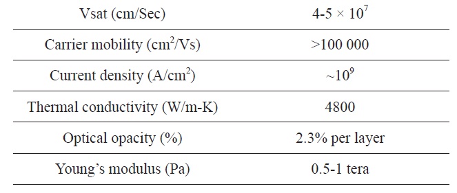
For radio-frequency (RF) electronic applications being considered, graphene exhibits the highest carrier mobility: >100 000 cm2 V-1 s-1 at room temperature [16]. This is not only ~100 times greater than that of Si, but about 10 times greater than state-of-the-art semiconductors lattice-matched to InP, currently regarded the best high-speed materials. The saturation velocity (vsat) of graphene has not been determined clearly yet, but it is estimated to be ~5 times greater than that for Si metal-oxide semiconductor field-effect transistor (MOSFETs) [17]. With expected large on-state current density and transconductance per gate capacitance compared to Si, graphene has the potential to offer excellent switching characteristics (capacitance/ on-state current) and short-circuit current gain cut-off frequency [18]. Although it is too early to predict, graphene-on-Si FETs [19] could potentially be further developed and processed in a manner compatible with Si complementary MOS (CMOS) with desirable integration density for system-on-chip applications.
While there are numerous challenges to be overcome for graphene to become a mature
[Table 1.] A brief summary of properties of graphene

A brief summary of properties of graphene
technology, this material offers unique device and potential circuit applications ranging from conventional unipolar RF electronics, such as low-noise amplifiers (LNAs), to unique ambipolar RF electronics such as frequency multipliers, mixers and high-speed radiometers. With observed constant device transconductance over the gate voltages [20], graphene FETs could potentially offer LNAs with higher dynamic range per given DC power, beyond the antimony-based low-bandgap devices. With graphene FETs biased near the ambipolar point, graphene FETs behave close to ideal “square-law” devices near the ambipolar point i.e., I(Vg) ∝ Vg 2, where Vg is the gate voltage. It would greatly suppress odd-order harmonics and/or third-order intermodulation products and improve dynamic range in communications.
2. Status of Epitaxial Graphene-on-SiC Transistors
Graphene FETs are being developed on the wafer-scale utilizing graphene-on-Si [19,21], graphene-on-SiC [20,22-24], and graphene transferred to SiO2 substrates [25]. Several promising device parameters have been demonstrated. For example, epitaxial graphene RF FETs have been demonstrated in a top-gated layout with the highest ever on-state current density of 3 A/mm [24]. On the other hand, the current-voltage characteristics are quasi-linear with weak saturation behaviors, yielding low transconductance (gm) per capacitance (i.e., <140 mS/mm at 3.4 fF/ μm2) and poor voltage gain (transconductance /output conductance). Also, the ratio of on-state current over off-state current, Ion/Ioff, was ~4 with field-effect mobility below 200 cm2/Vs. While graphene field-effect mobility as high as 5400 cm2/Vs for electron has been demonstrated [22], it was achieved using six to seven layers of epitaxial graphene on C-face SiC substrates,
resulting in an Ion/Ioff ratio of <2. In the case of graphene FETs fabricated on the Si-face of SiC substrates, field-effect mobility has been limited to below 1200 cm 2/Vs, but with an improved Ion/Ioff ratio of ~10 [23].
Top-gated graphene n-channel FETs (n-FET) and p-channel FETs (p-FETs) from epitaxial graphene layers were demonstrated with excellent I-V saturation behaviors [20] with a record peak extrinsic transconductance of 770 mS/mm. Also, the effective mobility and field-effect mobility versus Eeff were characterized and compared with Hall mobility. The epitaxial graphene layers were grown on Si-face 6H-SiC substrates on 75-mm wafers via Si sublimation [26]. The sheet electron carrier density of the epitaxial graphene layer was typically 8.8 × 1012 cm-2 at room temperature and had electron mobility of ~1192 cm2/Vs, characterized by non-contact Hall Lehighton 1600. The number of epitaxial graphene layers was found to be one layer on the SiC terraces and two layers on the step edges over the entire 75- mm wafer as characterized by Raman analysis and transmission electron microscopy analysis.
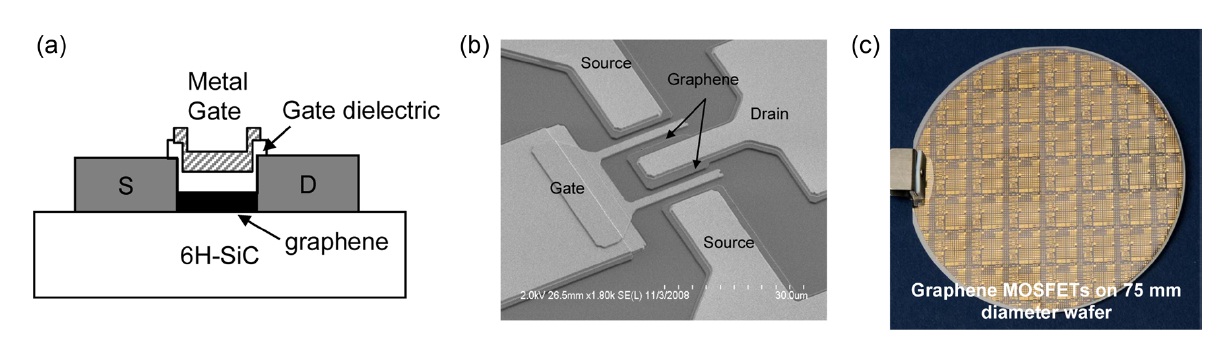
Figs. 1a-c shows the graphene FET processed in a layout, where the gate metal is aligned with respect to the ohmic metals in an under lap layout with a gate-to-source/drain separation of <100 nm to minimize the access resistance over a source-drain spacing (Lsd) of 1 μm. The source access resistance was <0.2 Ω·mm via the standard end-point measurements on transmission line method structures. A graphene channel width of 6 μm was defined by O2 plasma etching. The metal gates were processed with Ti/Pt/ Au metal deposition and lift-off process on top of a 35-nm-thick SiO2 gate dielectric layer deposited by electron beam evaporation. The gate leakage current was in the range of ~nA/μm2 or less, which is negligible in the device characterization presented here.
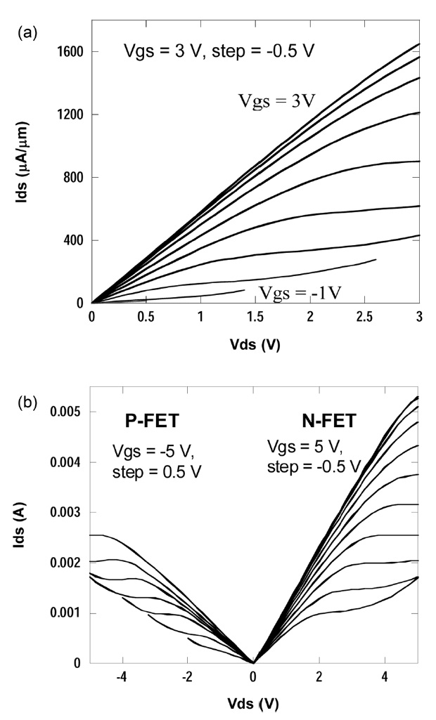
Figs. 2a and b shows the measured room temperature and the common-source current-voltage characteristics of a two-gate finger 6-μm-wide n-channel graphene FET (denoted as 2f × 6 μm), in which excellent drain current saturation was observed. The source-to-drain voltage (Vds) increased to 3 V, where the gate-to-source (Vgs) voltage was stepped from 3 V (top-curve) in steps of -0.5 V. At Vds = 1 V, on-state current at Vgs = 3 V was 590 mA/mm. The Ion/Ioff ratio was ~13. At Vds = 0.5 V, the Ion/Ioff ratio increased to 20. At Vds = 3 V, the on-state current at Vgs = 3 V was measured as high as 1650 mA/mm. The onresistance was 1.6 Ω·mm. The peak extrinsic gm of 770 mS/ mm was measured at Vds = 3.05 V, which is the highest ever, amongst epitaxial graphene FETs.
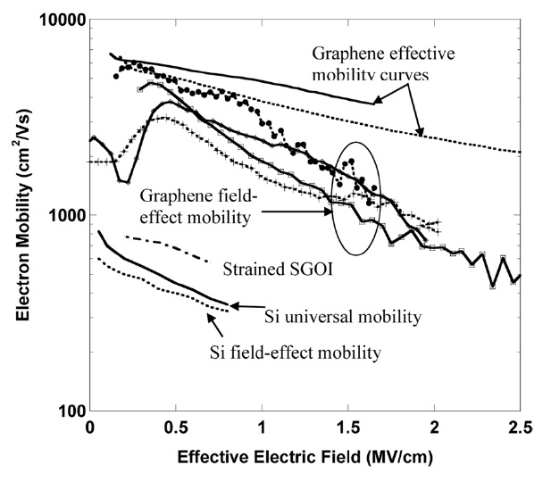
Fig. 3 shows extracted effective mobility (μeff) and field-effect mobility (μFE) of graphene n-FETs versus the effective electric field, Eeff. In comparison, the universal and field-effect mobility of Si n-MOSFETs [27] and strained Si n-MOSFETs on SiGe-onoxide [28] are shown. While both the μeff and μFE of the graphene n-FETs depend on Eeff, both values were higher than 1000 cm2/Vs over a wide range of the effective electric field up to 1.6 MV/cm. The peak field-effect mobility values ranged from 3200 cm2/Vs to 6000 cm2/Vs. A record field-effect mobility of 6000 cm2/Vs was obtained at an effective electric field of 0.27 MV/cm. The measured field-effect mobility of graphene n-FETs was at least seven times higher than that of Si n-MOSFETs in international technology roadmap for semiconductor and ~80 times higher than ultra-thin-body SOI n-MOSFETs. The peak field-effect mobility of graphene p-FETs was also determined to be 3200 cm2/Vs at an effective electric field of 0.2 MV/cm.
3. Graphene FET RF Performance
Regarding the graphene FET speed performance, in 2009 an extrinsic current-gain cutoff frequency (ft ) and maximum oscillation frequency (fmax) of 4.2 GHz and 14 GHz was reported with a 2 μm gate length [24]. The speed performance was not optimized due to the overlap capacitance between the gate and ohmic metal pads. In 2010, graphene FETs with a 240 μm gate length reported de-embedded ft/fmax of 100 GHz/10 GHz, while there is no extrinsic ft/fmax reported [29]. With graphene FETs processed with self-aligned nanowire gate with a gate length of 140 nm, de-embedded ft of 300 GHz was claimed while the extrinsic ft of 2.4 GHz was measured [30].
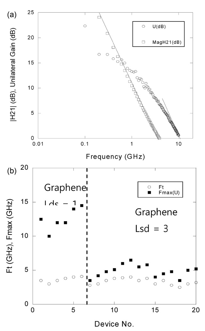
As an example of graphene FET RF performance, Fig. 4a shows the measured magnitude of H21 (|H21|) and Mason’s unilateral gain (U) of the 2 × 12 μm graphene FETs with sourcedrain spacing (Lds) of 1 μm. The S-parameters were measured at Vds = 5 V and Vgs = -2.5 V. An extrinsic ft of 4.1 GHz was extracted, yielding an extrinsic ft·Lg of 8.2 GHz·μm. The extrinsic gm was 195 mS/mm. A fmax of 11.5 GHz was extracted from the unilateral gain with a slope of -20 dB/decade. Fig. 4b shows a plot of extrinsic ft and fmax measured from the graphene FETs. For graphene FET with Lds = 3 μm, the extrinsic gm improved to 148 mS/mm at Vds = 9 V, yielding the extrinsic ft and fmax of 4.4 GHz and 6 GHz, respectively. For graphene FET with Lds = 1 μm, the ft and fmax were 4.2 GHz and 14 GHz, respectively, at Vds = 7 V. With a source access resistance of 1.9 Ω·mm, the intrinsic gm becomes 205 mS/mm. This yields an intrinsic ft of 5 GHz with an intrinsic ft·Lg of 10 GHz·μm, which is slightly better than 8.9 GHz·μm from the bulk Si NMOS.
At present, the RF performance of graphene FETs is not close to what had been predicted by the intrinsic saturation velocity of the graphene channel, 4-5 × 107 cm/sec. The theoretical carrier transport velocity provides ft·Lg product >50 GHz·μm, which is far from the currently observed values of ft·Lg products. The ft·Lg product of graphene FETs is expected to improve as the quality of the epitaxial graphene film, gate dielectric layer, transconductance, and transistor fabrication processing improves with reduced parasitic charging delay [31].
In most RF applications, fmax is very important to provide amplifiers with gain. The weak I-V saturation leads to a smaller
output resistance (Rds), transconductance, and higher Cgd compared to other semiconductor FETs with a finite bandgap. In order to maintain high fmax in short channel graphene FETs, channel engineering to reduce band-to-band tunneling will be desired as a mitigation method.
4. Graphene FET Ambipolar RF Applications
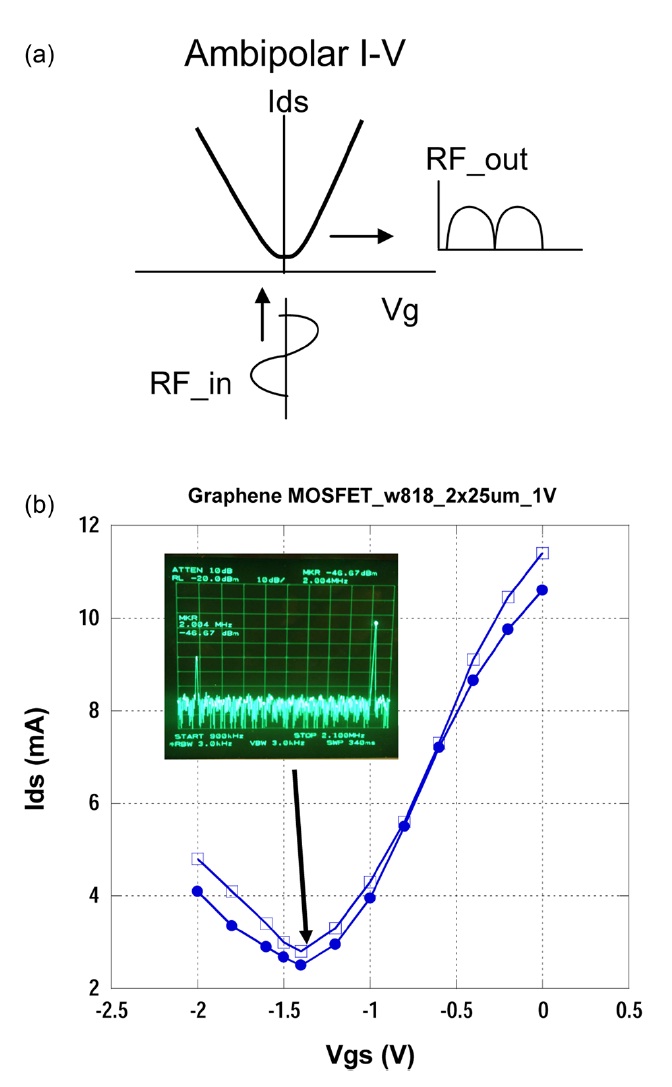
Unlike Si, SiGe, and III-IV semiconductor materials, graphene has a unique ambipolar characteristic, where excellent field-effect mobility for both electron and holes can be obtained. For instance, field-effect mobility of 6000 cm2/Vs for electrons and 3200 cm2/Vs for holes was obtained [20]. Several potential applications for these unique ambipolar graphene FETs have been under evaluation [32-34]. These include frequency multipliers, mixers, and oscillators. Frequency multiplication or mixing is based on the nonlinearity of graphene FETs near the ambipolar point.
If graphene FETs behave as ideal “square-law” devices near the ambipolar point ie., I(Vg) ∝ Vg 2, it would greatly suppress odd-order harmonics and/or third-order intermodulation products and improve dynamic range in communications. A suppression of odd-order signals (f, 3f, 5f…) compared to the second harmonic (2f) was shown in the frequency multiplication experiments up to 200 kHz with ~10 dB suppression [32,33], and above GHz [34].
Fig. 5a shows a schematic of the frequency multiplication process in the case of ambipolar transfer curve. Fig. 5b shows an example of measured RF output spectra consisting of strong even-order harmonic signals with odd-order harmonics suppressed by >25 dB, supporting “square-law” device operation at the ambipolar point.
The phase noise measurement was reported with a carrier-tonoise degradation of 6 dB, which implies noiseless frequency multiplication without additional 1/f noise up-conversion during the nonlinear process [34]. Capitalizing on the ambipolar nature of graphene FETs, ambipolar mixers were demonstrated in the GHz range [35,36]. The conversion loss is typically in the order of 20-30 dB, which has to be solved in order to make ambipolar frequency doublers and mixers competitive technologies.
While it is early in the stage of development to clearly forecast its impact, graphene FETs could potentially offer performance benefits in RF systems including LNAs, frequency multipliers, mixers and high-speed radiometers. The future success of the RF circuit applications depends on high-quality material growth on large-wafer scale, vertical and lateral scaling of graphene MOSFETs to minimize parasitics and improved gate modulation efficiency in the channel, a bandgap engineering of graphene channels in the MOSFETs, and innovative circuit concepts.