검색 전체 메뉴
PDF
맨 위로
OA 학술지
Characteristics of Hafnium Silicate Films Deposited on Si by Atomic Layer Deposition Process
  • 비영리 CC BY-NC
  • 비영리 CC BY-NC
ABSTRACT
Characteristics of Hafnium Silicate Films Deposited on Si by Atomic Layer Deposition Process
KEYWORD
Metal-oxide-semiconductor capacitor , Atomic layer deposition , high-k , HfSixOy , Interfacial layer regrowth , O2 annealing
  • 1. INTRODUCTION

    Several candidates for future high-k gate oxides in metaloxide-semiconductor (MOS) devices have been extensively studied by many research groups to overcome the problems such as the large leakage current caused by the direct tunneling through extremely thin SiO2. Hafnium-based oxides are under intense investigation to replace conventional SiO2[1-3]. Recently, research efforts on high-k gate oxides have been focused on materials such as HfO2, and its silicates due to their excellent electrical properties and high thermal stability in direct contact with Si[1-5]. HfO2 has attracted considerable attention and has been considered as one of the most promising high-k candidates due to its high dielectric constant (~25), reasonable band alignment and relatively large band gap of 5.65 eV [1]. However, amorphous HfO2 can easily crystallize at relatively low temperatures (~500℃):Crystallization not only increases the leakage current, but also deteriorates the interface of high-k oxide and Si substrate [1-5].

    Low-temperature deposition and oxidation may be used in an attempt to prevent the crystallization of high-k oxide. It is,however, likely that the thermal cycles required in fabricating a transistor could cause high-k oxide to crystallize. Although the dielectric constant values k of HfSixOy (~13) is substantially lower than that of HfO2, the structure of HfSixOy remains amorphous even after the high temperature heat treatment. Therefore, it is possible to minimize the leakage current through the grain boundaries in HfSixOy[2-5]. HfSixOy films have been deposited by pulsed laser deposition (PLD) [6], sputtering [3], E-beam evaporation [5], chemical vapor deposition [7] and atomic layer deposition (ALD) [8]. PLD and the sputtering process have some drawbacks such as poor step coverage and the damaging effect of the plasma on the channel region of the CMOS devices [9]. ALD is generally preferred for depositing very thin films because it is based on self-limiting surface reactions, which gives it attractive properties, like accurate and simple control of the film thickness and composition, sharp interfaces, highly conformal, uniform thin film growth, good reproducibility, and high film qualities at relatively low temperatures [10]. However, it has been reported that the residual metal components caused by insufficient oxidation during the ALD process may cause the C-V hysteresis and leakage current generation [11].

    2. EXPERIMENTS

    The HfSixOy films were deposited by the ALD method on the p-type Si substrate at 450℃. Prior to the deposition of HfSixOy film, the Si wafers were treated in a buffered HF (HF:H2O =1:100) solution to remove native oxide and contaminants. The precursors used in this work were Hf[OC(CH3)2CH2OCH3] and Si[OC(CH3)2CH2OCH3] at a ratio of 75:25% and remote-plasma oxygen with carrier N2 gas. The remote-plasma oxidation has been demonstrated to reduce the amount of impurities, thus improving the electrical properties [11]. The processing parameters were set to obtain a final thickness of 35 A. During the ALD process,the pressure of the reactor was kept at 100 Pa. After completing the deposition cycles, the HfSixOy films were annealed at various temperatures (i.e., 500℃, 700℃ and 900℃) using a rapid thermal processor (RTP) in O2 ambient for 5 minutes. After O2 annealing, Pd (1,000 A) was thermally evaporated through a shadow mask to fabricate the MOS capacitors. The metal gate area was 2.4 × 10⁻⁴ cm2. The effects of the annealing process were analyzed by high-resolution transmission electron microscopy(HR-TEM), X-ray photoelectron spectroscopy (XPS), capacitance versus applied voltage (C-V) and leakage current-density versus applied voltage (J-V) measurements. The capacitance was measured using a HP4275A LCR meter at the frequency of 1 MHz.The leakage current density characteristics were monitored using a HP4145B semiconductor parameter analyzer.

    3. RESULTS AND DISCUSSION

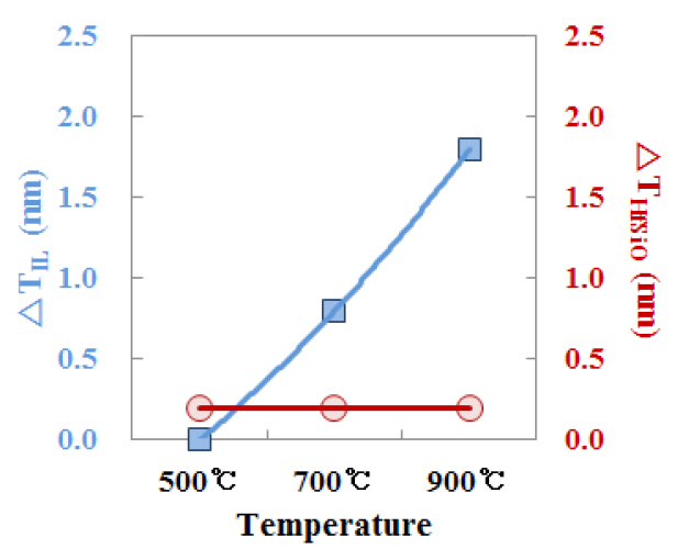
    Figure 1 shows regrowth of interfacial layer (IL) and HfSixOy following O2 annealing. Thicknesses were measured by HR-TEM.Initial thicknesses of IL and HfSixOy were 1.6 nm and 2.4 nm,respectively. The data shown in Fig. 1 were obtained from the samples subjected to the post deposition annealing using RTP in O2 ambient for 5 minutes at 500℃, 700℃ and 900℃, respectively.

    While the IL thickness increased as the annealing temperature increased, the thickness of the HfSixOy layer (with the exception of IL between Si substrate and HfSixOy layer) shows no visible change after annealing at high temperature. The HfSixOy film is completely amorphous at 500℃ and 700℃. In contrast, in the HfSixOy film with 900℃ annealing, we observed crystallized portions.Recently, it was reported that localized crystallization occurs after a high temperature annealing [12-14].

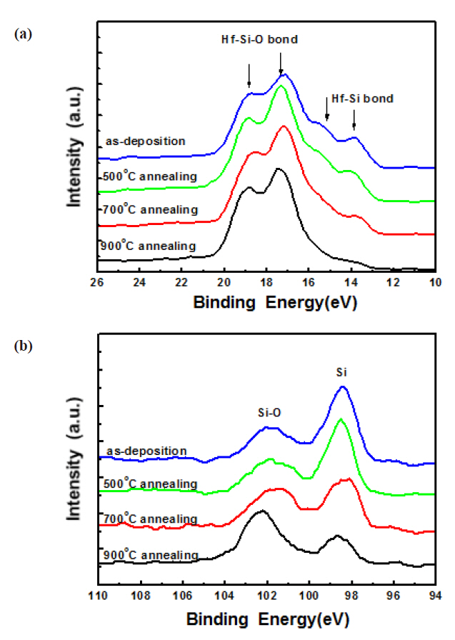
    In order to examine the structural change associated with the

    annealing temperature, we measured the XPS spectra of the asdeposited HfSixOy film and annealed HfSixOy (Fig. 2). Figure 2 exhibits the (a) Hf 4f and (b) Si 2p spectra observed from HfSixOy layer annealed with variable temperature by RTP. Figure 2(a)shows the Hf 4f(7/2) peak at 19.1 eV, separated by 1.7 eV from the Hf 4f(5/2) peak at 17.4 eV, which is attributed to Hf bound to oxygen[12]. From Si 2p peak in the Fig. 2(b), we observed that the higher the temperature, the larger the silicate peak associated with Si-O bonding [15]. On the other hand, as shown in Fig. 2(a),in the Hf 4f peak, the identified shoulders that appear in the lower binding energy are considered to be caused by an unoxidized Hf-Si bond. However, as the annealing temperature increased,the residual Hf-Si peaks disappeared. This implies that the metallic Hf components are oxidized by diffusion of oxygen from the surface into the Si substrate, in the oxygen gas annealing [12].This is also associated with an increase in the IL thickness between the Si substrate and HfSixOy layer. The physical changes in the IL have an effect on the electrical properties.

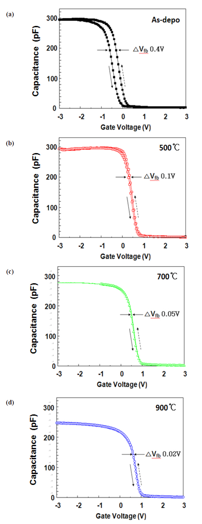
    Figure 3 shows the capacitance versus applied voltage (C-V)characteristics of the p-Si/HfSixOy/Pd capacitor according to annealing temperature. From Fig. 3, we find that the accumulation capacitance decreases as the annealing temperature increase.This phenomenon can be explained by the increase in the IL thickness due to high temperature annealing, as shown in Fig.2. The as-deposited HfSixOy films exhibit a large hysteresis of around 0.4 V due to the defects caused by partial oxidization(Hf-Si bonding states). The hysteresis voltages were reduced by a higher annealing temperature. These experimental results indicate that the charges trapped in the film decreased with O2 annealing.

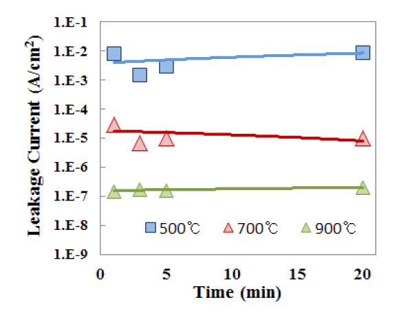
    Figure 4 shows the leakage current density characteristics of

    the p-Si/HfSixOy/Pd capacitor according to annealing temperature.The leakage current is dependent on annealing temperature.

    For example, we obtained the lowest value of leakage current

    density from an annealed sample at 900℃ due to the increase in the IL thickness. The leakage current density of HfSixOy film annealed at 500℃ is similar to that of the as-deposited sample.Moreover, both samples have nearly the same capacitance value.

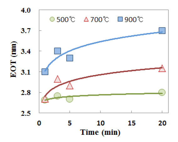
    Figure 5 shows equivalent oxide thickness (EOT) characteristics of p-Si/HfSixOy/Pd capacitor according to annealing temperature and time. EOT was dependent on annealing temperature.

    EOT and the leakage current density of the HfSixOy film is less dependent of the post deposition annealing time, as shown in Figs. 4 and 5. As the annealing time increases, both the EOT and leakage current density show only a little change. This result indicates that the relationship between the electrical characteristics and annealing condition is more strongly dependent on the annealing temperature than the annealing time.

    4. CONCLUSIONS

    We have studied the effect of annealing on HfSixOy film deposited by ALD. We found that post deposition annealing causes oxidation of residual Hf metal components, resulting in an improvement in the hysteresis window and leakage current density.These experimental results indicate that the post deposition annealing improves the electrical and physical characteristics (e.g.,hysteresis window and leakage current were decreased). In addition, we found that the role of annealing temperature is more important than that of annealing time in post deposition annealing.However, EOT increased as increasing the temperature due to IL regrowth. Based on the current observation, the annealing temperature has to be carefully controlled to minimize the growth of interfacial oxide, which degrades the value of the EOT.

참고문헌
  • 1. Wilk G. D, Wallace R. M, Anthony J. M 2001 [J. Appl. Phys.] Vol.89 P.5243
  • 2. Kim H. D, Roh Y, Lee Y, Lee J. E, Jung D, Lee N. E 2004 [J. Vac.Sci. Technol. A] Vol.22 P.1347
  • 3. Wilk G. D, Wallace R. M 1999 [Appl. Phys. Lett.] Vol.74 P.2854
  • 4. Watanabe H, Saitoh M, Ikarashi N, Tatsumi T 2004 [Appl. Phys.Lett.] Vol.85 P.449
  • 5. Wilk G. D, Wallace R. M, Anthony J. M 2000 [J. Appl. Phys.] Vol.87 P.484
  • 6. Zhu J, Liu Z. G, Feng Y 2003 [J. Phys. D: Appl. Phys.] Vol.36 P.3051
  • 7. Zhu J, Liu Z. G, Feng Y 2004 [J. Cryst. Growth] Vol.263 P.442
  • 8. Duenas S, Castan H, Garcia H, Barbolla J, Kukli K, Ritala M, Leskela M 2005 [Spanish Conference on Electron Devices] P.45
  • 9. Kim W. K, Kang S. W, Rhee S. W, Lee N. I, Lee J. H, Kang H. K 2002 [J. Vac. Sci. Technol. A] Vol.20 P.2096
  • 10. Kim J, Yong K 2005 [J. Electrochem. Soc.] Vol.152 P.F45
  • 11. Yamamoto K, Hayashi S, Niwa M, Asai M, Horii S, Miya H 2003 [Appl. Phys. Lett.] Vol.83 P.2229
  • 12. Yamaguchi T, Iijima R, Ino T, Nishiyama A, Satake H, Fukushima N 2002 [IEDM Tech. Dig.] Vol.621
  • 13. Yamaguchi T, Ino T, Satake H, Fukushima N 2003 [41st Annaul IEEE International Reliability Physics Symposium Proceedings] P.34
  • 14. Visokay M. R, Chambers J. J, Rotondaro A. L. P, Shanware A, Colombo L 2002 [Appl. Phys. Lett.] Vol.80 P.3183
  • 15. Punchaipetch P, Pant G, Quevedo-Lopez M. A, Yao C, El-Bouanani M, Kim M. J, Wallace R. M, Gnade B. E 2004 [IEEE J.Sel. Topics. Quantum Electron.] Vol.10 P.89
OAK XML 통계
이미지 / 테이블
  • [ Fig. 1. ]  Interfacial layer regrowth in terms of O2 annealing temperature.
    Interfacial layer regrowth in terms of O2 annealing temperature.
  • [ Fig. 2. ]  X-ray photoelectron spectroscopy spectra at (a) Hf 4f and (b)Si 2p spectra annealed by rapid thermal processor at 500℃ 700℃and 900℃ respectively for 5 minutes in O2 ambient.
    X-ray photoelectron spectroscopy spectra at (a) Hf 4f and (b)Si 2p spectra annealed by rapid thermal processor at 500℃ 700℃and 900℃ respectively for 5 minutes in O2 ambient.
  • [ Fig. 3. ]  High frequency capacitance (C-V) characteristics of p-Si/ Hf-SixOy/Pd capacitors annealed by rapid thermal processor at 500℃700℃ and 900℃ respectively for 5 minutes in O2 ambient.
    High frequency capacitance (C-V) characteristics of p-Si/ Hf-SixOy/Pd capacitors annealed by rapid thermal processor at 500℃700℃ and 900℃ respectively for 5 minutes in O2 ambient.
  • [ Fig. 4. ]  Equivalent oxide thickness of p-Si/HfSixOy/Pd capacitors annealedby rapid thermal processor at 500℃ 700℃ and 900℃ respectivelyfor 5 minutes in O2 ambient.
    Equivalent oxide thickness of p-Si/HfSixOy/Pd capacitors annealedby rapid thermal processor at 500℃ 700℃ and 900℃ respectivelyfor 5 minutes in O2 ambient.
  • [ Fig. 5. ]  Equivalent oxide thickness of p-Si/HfSixOy/Pd capacitors annealedby rapid thermal processor at 500℃ 700℃ and 900℃ respectivelyfor 5 minutes in O2 ambient.
    Equivalent oxide thickness of p-Si/HfSixOy/Pd capacitors annealedby rapid thermal processor at 500℃ 700℃ and 900℃ respectivelyfor 5 minutes in O2 ambient.
(우)06579 서울시 서초구 반포대로 201(반포동)
Tel. 02-537-6389 | Fax. 02-590-0571 | 문의 : oak2014@korea.kr
Copyright(c) National Library of Korea. All rights reserved.